DDS Function generator

This has been on my list of things to do for a while and represent a few challenges. Chips like AD9851 contains a full DDS that interface to a MCU on one side and give 3.3V signals on the other side. I have yet to decide wherever  to use AD9851 or something else, butAD9851 is the candidate as we speak.

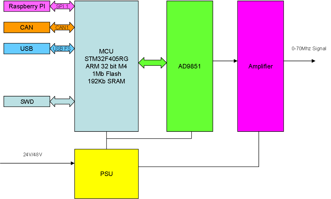
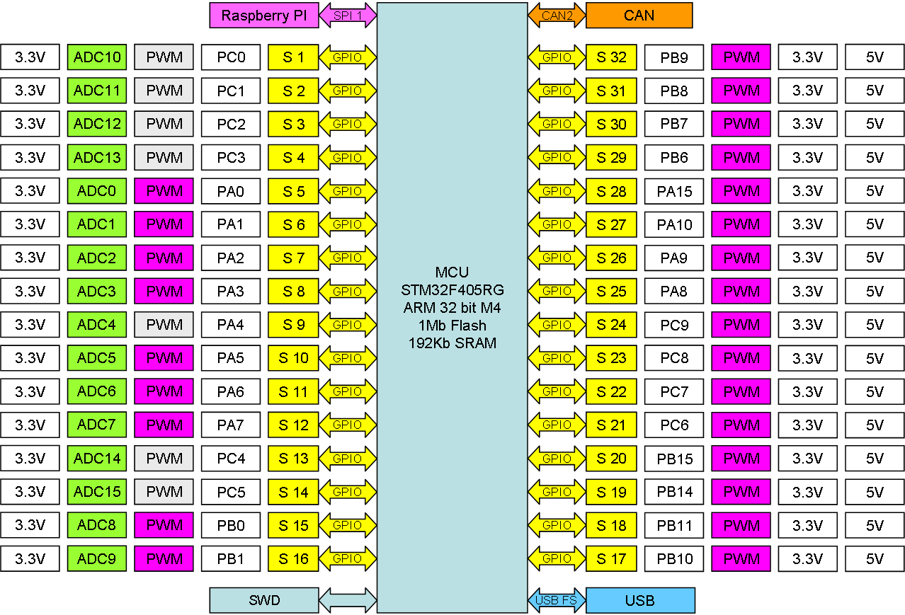
The block diagram above outline the functionality of the DDS. The first part a MCU  and AD9851 is straight forward. I have not used AD9851, but I have breakout boards + loads of reference schematics to work on. If nothing else I will make a Hat with 1 x 3.3V out channel. In many cases that is all that is needed and with my capability to stack up Hat’s we already talk about a very nice instrument.

The PSU is straight forward. I use 24 or 48V to create +/- 12 or 24V out as base. The amplifier is however far from straight forward.

First step is to offset the 3.3V signal, the second to amplify it and remember that we talk about signals up to 70Mhz. The Hat might get crowded, so it is possible that I need to split this onto 2 Hats and as such also accept that the amplifier only support 1Mhz or something.

I have dreaded this project a little because I only was on 2 layer designs, but as I now have moved to KiCAD and 4 layers or more is possible I want to give it a go. I think the first step is to make schematics for MCU and AD9851 as well as playing around with my breakout boards a little.

The primary usage for this is test equipment and it’s fun to make your own, but most important fun to have this as a component in my modular system.

KiCAD 3D Packages

I must admit that the realism in KiCAD’s 3D model is growing on me, it is great for precentations in here. Adding a 3D package was about selecting an associated 3D model file, so from now on I saved a copy of this footprint with the associated model in my own extension library.

Adding drill holes was easy – it actually is a component selection in the library, so all I needed to do was to select the correct one and set dimesions/position. On these drawings I had to switch off realistic mode on the backside to actually see drill hole areas properly.

One advice is that KiCAD actually crash from time to time. It crashed as I tried to remove the old via’s, but I opened the file in a text editor and removed the objects manually.

Target 3001 had a script option to make your own 3D packages. Basically you have the same in KiCAD since files look like scripts. But, the better way is to use some 3D design tool that can save in the correct format.

As for the 32xServo/IO – I could only find the SMD version of the 1.27 pich JST connectors (CAN port) and they are a bit wider. I am not sure about this choise, but I will try them out. I need to find or make angled pin-headers 3 row deep and 2 more packages. I would also like to tilt a few things 45 degrees and add text, but other than that I am done – I have basically made my first prosjekt in KiCAD.

I have to credit the community for all the available youtube videos on various subjects – without those this would have been a much harder learning curve. My next task is to start making the boards on 4 layers. We are actually setting up our own assembly factory a few miles away from my lab. That said, I am not sure how to deal with production yet – it is down to logistics and even if I can assemble low cost I still have to ship units out. The later cost to much from Norway, but that is a different story.


32xServo/IO Hat Rev 1.4 Annotated

2nd Draft of my new 32xServo/IO Hat rev 1.4. Added the leds and missing SPI resistors + reorganized connectors at bottom. I notice that I need to add a capacitor to assist D2 (TVS) on the bottom + I want to add 2 jumpers allowing left and/or right array to be connected to 5V as supply +++ but, I am in no hurry to order this. As mentioned before I still have not fully tested rev 1.0 and it is mostly cosmetic changes. But, this has an obvious change that I put all analogue capable channels at left and all PWM only at right + to more care to use as many HW timer channels as possible. In the end I managed to grab 25 Hardware timer signals, leaving only 7 for SW bit banging.

  1. CAN 120 Ohm terminal jumper.
  2. CAN Port.
  3. 16 x Anague capable Servo/IO channels.
  4. USB Port. Great for development and stand-alone operation from PC as well as downloading new firmware.
  5. Servo power Connector.
  6. Leds 1 Power Led and 2 MCU leds.
  7. 16 x PWM only channels.
  8.  8 x 4 channel 5V TVS to protect MCU ports.
  9. 4 x drill holes in Raspberry PI 2 position/size.
  10. SWD connector.
  11. Raspberry PI 2,3,4 Connector.
  12. Led for CAN port indication.


This block diagram show the actual channel per channel capacity and what MCU signal I used as base.

My challenge now is how to order a PCB? As mentioned before Norwegian import rules changes 1.Jan.2020, so I get slammed 20.- USD on a 10.- USD order. I need to find ways to avoid those handling fees, but it will take time before sellers abroad adjust and start declaring Norwegian MVA. If Elecrow declare MVA I would pay 2.5 USD for a 10.- USD order, if they don’t I end up paying 2.5 USD in VAT + 20.- USD in handling fee. One solution is that I wait and order many PCB’s together because the handling fee is the same. Doing this on PCB is doable, but on components it is close to impossible. The drawback is that samples will start costing 3-4 times if I can get them at all. Don’t worry, you will hear me whining about this for some time until I find a solution.

32xServo/IO Rev 1.4

First draft of 32xServo/IO Hat. Designed withh KiCAD this time, but still a 2 Layer design. I lack 3D packages for Power connector, USB port, JST CAN port and Q1 Crystal. The Q1 Crystal footprint was my first footprint design, but is was rather straight forward. Next I will have to try adding a 3D package. The 3D model uses “Raytracing” and option in KiCAD to make the board look more realistic. You can see the ordinary 3D model below and make up your own mine. A 3D model is a 3D model, it has a functional purpose so I must admit I prefer the one below because it is faster – much faster to work with. But, it is nice to have options.

And yes – leds are missing. In fact many of the changes I discussed before needs to be inserted in the next draft.

Changing footprint and 3D model on Target 3001 was done in a proprietary scrip language that had its sides. My main challenge was that it took time and you forgot the script language between every time you used it + it was not well documented. Making footprint in KiCAD was very visual and straight forward – time saving.

KiCAD – PCB Layout

One of many new features that was not available in Target 3001 is display of signal names on tracks and pads. I selected the wrong footprint for SWD, but as it is the same size as a 1.27 pitch header I did not think it matter before I noticed that it count the pin differently – wherever this bug is in schematics or selected footprint can be discussed. What is important is that KiCAD allow me to see it.

Another feature is the capability to drag entire sections of lines to make room for a new one- The level of semi-automation on KiCAD is really impressive. I am actually routing manually, but the automation allows me to move earlier content to make space and suggest alternative routes from where I am with such an ease that PCB routing is done in a fraction of the time I needed with Target 3001 – and I considered Target 3001 to be easy to work with.

This is still a 2-layer layout for now as I am learning KiCAD properly the only way it can be done – by using it and gaining experience. But, I have not used the backside much at all do to the routers capability to find or make paths. It will obviously take a few weeks before I truly master KiCAD and I will not spam this blog with details – I think most of you get the picture by now – KiCAD was something I should had started on years ago! That said – getting started with KiCAD is a bit heavy so you must set your mind and start digging in watching videos and try and fail. KiCAD has to be learned the hard way, but it is worth it.

As for suggestions on how to improve KiCAD – don’t worry, I have plenty. The first I would start with is to merge the two screens that (1) allow you to watch footprint and (2) allow you to select footprint because the first let you see the footprint while the second don’t – luckily I van have both open at the same time because it’s a bit hard not seeing the footprint you select. But, again – you don’t want to hear about how I had to do this earlier + yes it’s a button to open a 3rd window where you can see the selected footprint 🙂

Looking at the backside pic above I notice how little I have used the backside – which is good since we are on 2-layer, but I also notice that I still have to learn how to deal with drill holes yet. One thing at the time.

The last think I wanted to show you is the semi-auto router. As you select two points on the PCB KiCAD will attempt to autoroute that lane. In this case I was more impressed that it actually found a path – I will not be using this one, but many times I do and end up routing much more single layer than before. I can now draw part of the lane manually by clicking on connection points and the auto-router will take it from there. And you can always use the drag function to optimize path afterwards as well. This is a big time-saver compared to how my previous tool worked. I assume it exist a full auto-router as well, but I have not tried that one yet.

Thanks for reading my early morning ranting…

Ordering new PCB’s

It is soon 1.jan.2020 and Norwegian import rules changes, meaning I basically get MVA and a 20.-USD handling fee on every package unless I get the foreign company to declare MVA. It will be a pain and take some time before this happens. Ordering parts from Asia will be close to impossible unless you order big quantities. It feels like my country are reverting back to the stone age…

2-Screens in use w/KiCAD

This is a screen-shot of my two screens. I have PCB router on left and schematics on right. As I work on PCB the schematics will show the associated part – neat little detail. KiCAD is actually multiple applications so its perfect to take full advantage of multiple screens as you work. I have routed 60% of the new board in about an hour – most times just playing around – KiCAD is so quick to route that it is amazing. The auto-router is also good at finding track options allowing me to stay as much as possible on the same layer + it’s a real pleasure to use via’s.

KiCAD 3D Model

This shows and early draft of rev 1.4 on KiCAD using their normal 3D model. KiCAD have a more realistic version that is a bit slower to draw, but for all poractical purposes it does the job. Accurate details is IMO not important here, the objective is to verify as much of the mechanics as possible. KiCAD enables export of images directly, but I ended up using my old trick of taking a screenschot and use Paint 3D.

What I am really happy with here is the PCB layout. Some things are a bit new and different yet, but the more I learn KiCAD the more I like it. on some features I seems to have less manual control than before, but all in all – setting this up was more about learning KiCAD than work.

As you can see I lack 3D model on 3 footprints + I have the wrong footprint on the crystal – I have yet to learn how to create my own 3D models and footprints. But, I am happy to see that the libraries contains far more + you get libraries from various sources. And yes I know – I am using straight headers rather than angled headers because I did not find angled headers 3 rows deep. I am not even sure if I actually used the correct tool for drill holes as what you see is a gigantic “via”, but I will get there thanks to hundreds of videos assisting me.

One of the tools I really appreciated is the measurement tools and aids on making correct dimensions – that was not existing in Target 3001.

Operating KiCAD feels like doing Schematics, PCB and 3D in one integrated tool. I know it is different tools, but once set up the next step is only a button away. It is a few manual steps between schematics and PCB to give you full control and I must admit I like having schematic symbols separated from footprints giving me options to replace footprint with a minimum of changes.

As for PCB routing – You have to remember that I started my carrier as Electronic Engineer back in 1978 using pen and paper to make schematics and PCB layout. Actually using a CAD tool is like putting someone used to a horse carry into a formula 1 car. Target 3001 impressed me, but getting used to KiCAD is like dropping into the cockpit of a jet-fighter. It’s semi- automatic routing is very impressive in terms of how fast you route. And just for the record – I have used Target 3001 for 4 years and KiCAD for 1 week. I still like Target 3001, but it is no match for KiCAD once you take the time needed to learn it’s user interface. And to remind you all – KiCAD is free, open source. It is C/C++ code with wxWidgets.

KiCAD vs Target 3001 – 2nd Impression

1 – Schematics – KiCAD is most definitly a step up. It is much, much faster to work with once you get used to the somewhat weird user interface.

2 – PCB Layout – It is hard to say. I see huge advantages in the life-cycle of interactions between PCB/Schematics as I apply changes.

3 – 3D – Both gets the job done. KiCAD have a special mode making 3D model look realistic, but so far I must admit that I preffer Target 2001 on this.

Will be interesting to see how these impressions change as I get to learn KiCAD more – so far it is ok – weird, but ok.

I am mainly a Windows user/developer so my expectations to user interface is standarized through years of Windows usage. Target 3001 fall into that category. People who have grown up with Linux is not used to this and tend to re-invent the wheel by doing things differently – KiCAD falls into this category. It takes a bit of time to get used to because it don’t follow standards we are used to. Once you get the shortcuts into your fingers they actually are quite convenient.

Making a LED Lamp

I am a bit handicapped as my Lamp with a magnifier broke. I was using that all the time, but having seen how badly designed that it I decided to rebuild both of my lamps to be LED lamps.

What I will do is to buy a 130VAC to 12VDC adapter in a shop (or use an old one laying around) that is CE aproved – and this is very important in Norway. I am allowed to deal with 12V, but if I deal with 230VAC and start a fire my insurance might kick back on me.

This project is straight forward – Use an adapter to get 12V and make a PCB that is a circle fitting inside the lamp with LEDS designed so they accept 12V – in reality that is 3 leds with a resistor in series.

The next step I am considering is to use an ESP32 and a few Half H-Bridges to dim different parts of the lamp to control light, but for now I will just make a dumb, analogue design on vero boards to get my lamp working again.