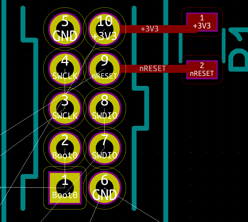
One of many new features that was not available in Target 3001 is display of signal names on tracks and pads. I selected the wrong footprint for SWD, but as it is the same size as a 1.27 pitch header I did not think it matter before I noticed that it count the pin differently – wherever this bug is in schematics or selected footprint can be discussed. What is important is that KiCAD allow me to see it.
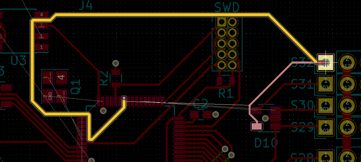
Another feature is the capability to drag entire sections of lines to make room for a new one- The level of semi-automation on KiCAD is really impressive. I am actually routing manually, but the automation allows me to move earlier content to make space and suggest alternative routes from where I am with such an ease that PCB routing is done in a fraction of the time I needed with Target 3001 – and I considered Target 3001 to be easy to work with.
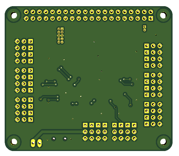
This is still a 2-layer layout for now as I am learning KiCAD properly the only way it can be done – by using it and gaining experience. But, I have not used the backside much at all do to the routers capability to find or make paths. It will obviously take a few weeks before I truly master KiCAD and I will not spam this blog with details – I think most of you get the picture by now – KiCAD was something I should had started on years ago! That said – getting started with KiCAD is a bit heavy so you must set your mind and start digging in watching videos and try and fail. KiCAD has to be learned the hard way, but it is worth it.
As for suggestions on how to improve KiCAD – don’t worry, I have plenty. The first I would start with is to merge the two screens that (1) allow you to watch footprint and (2) allow you to select footprint because the first let you see the footprint while the second don’t – luckily I van have both open at the same time because it’s a bit hard not seeing the footprint you select. But, again – you don’t want to hear about how I had to do this earlier + yes it’s a button to open a 3rd window where you can see the selected footprint 🙂
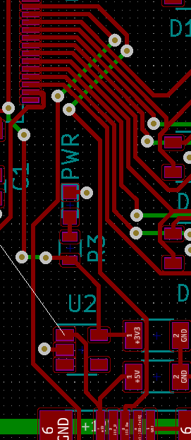
Looking at the backside pic above I notice how little I have used the backside – which is good since we are on 2-layer, but I also notice that I still have to learn how to deal with drill holes yet. One thing at the time.
The last think I wanted to show you is the semi-auto router. As you select two points on the PCB KiCAD will attempt to autoroute that lane. In this case I was more impressed that it actually found a path – I will not be using this one, but many times I do and end up routing much more single layer than before. I can now draw part of the lane manually by clicking on connection points and the auto-router will take it from there. And you can always use the drag function to optimize path afterwards as well. This is a big time-saver compared to how my previous tool worked. I assume it exist a full auto-router as well, but I have not tried that one yet.
Thanks for reading my early morning ranting…