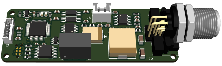
CCU (Central Control Unit) is the name I give units that contain the core “brain” and only communication IO. The module below is an example of the core of a CCU with 3 external CAN ports, 8 internal module ports and 2 external Links. This is a fast MCU with a decent amount of speed, SRAM and Flash + it has it’s own SPI Flash + a USB for debug only. The CAN ports are standard M12-5 A Code and wired according to a de-factor standard. These will be used for CAN and for RS485. Possible I can use B or D-code for RS485.

Links can be used for modules as well, but they are designed to be links to different CCU’s allowing them to be connected in series to extend the CCU or linked up as a redundant unit. The unit above takes 5V in, so it is dependant on a 24V PSU unit.
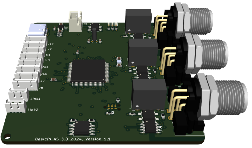
The board above can be used alone or connected to a range of IO modules with different capabilities to form a larger CCU or even a ECU (Electronic Control Unit). A system will usually have one CCU and multiple ECU’s, actuators and sensors. As a rule we use CAN on everything and only RS485 or Ethernet as an exception. We can also use RS232 and other techniques as needed.
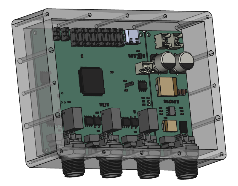
Each module is 70x25mm in size. The CPU module occupy 3 slots and each module can occupy as many slots as needed + they can double length to 140mm or even larger with special cabinets. The core is small project boxes that can be filled with modules as per need to form a custom PLC.
I use the term “PLC” because a modern PLC is mostly the same as above with specialized SW. My PLC languages will include C++, C#, Rust and Python + it will be supported by BSA. In reality I will be coding drivers in C++ and logic in PLD, but that is my choises – it should not limit you. The objctives is small size, plug and play and low development cost. In short you pay a few bucks for a few HW units, connect them together and will be up running in no time with a prototype or completed project.

This block diagram illustrate a CCU. A minimal CCU is only PSU + CPU module with 3 x CAN. A maximized box can contain up to 8 modules and as the MCU itself can act as a module it is basically no limit on how much you can put into a box.
CCU – Central Control Unit. Basically system level logic and communication.
ECU – Electronic Control Unit. Basically a box with a CAN connected to a CCU controlling electronics directly.