UML State Diagram

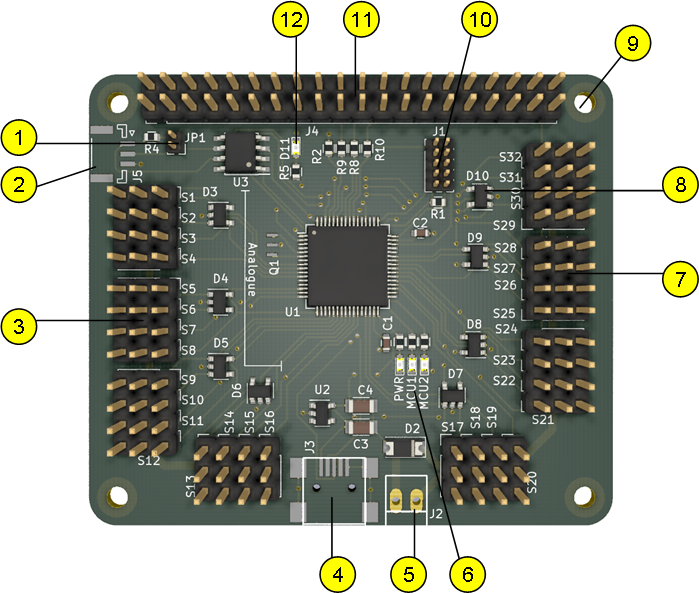
UML State Diagram is a standard, but I find it’s implementation into tools to be wage. So, I implement my own adaption because I intend to have a 1:1 with actual source code. This is not uncommon as most automation tools will have to make adaption in areas where executable accuracy is weak.

I was introduced to programming with UML State Diagrams through a different tool that I found to be of little use. But, it demonstrated the concept and I often use state diagrams so why not have one that actually is 1:1 with code on high level. A state diagram lack a lot of executable accuracy as it is only a high level diagram, but it does have some excellent qualities of showing event/signal driven flow on high level and as such accelerate overview of source code. The examples below are preliminary from an experimental tool.

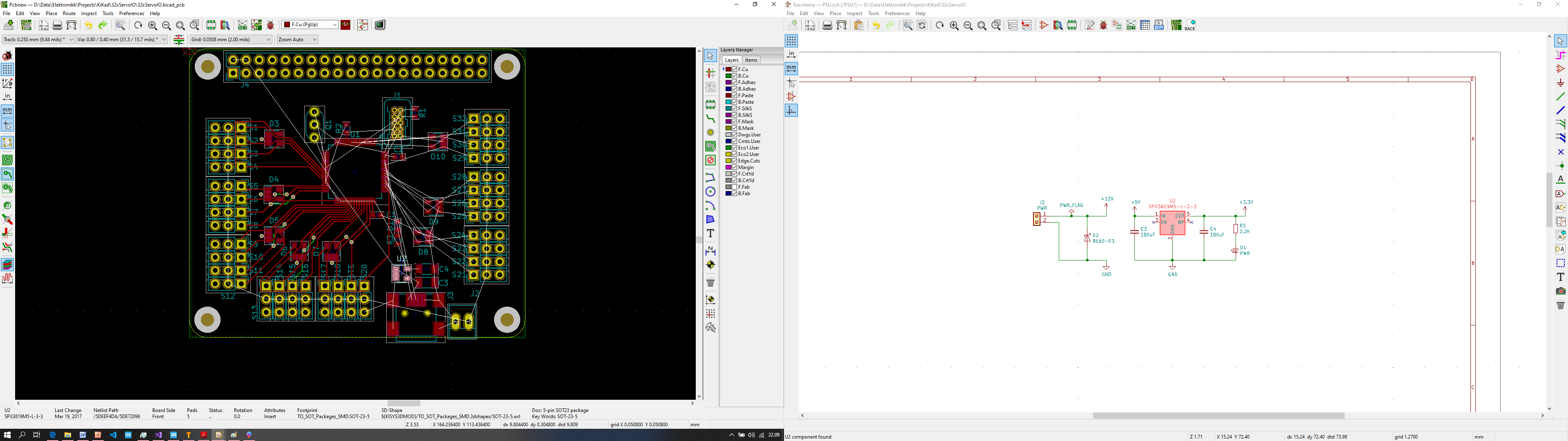
The first symbol I use is the Entry point – a simple circle with a single output connection point (the red dot). All events inthese examples have the name “Hello”. The Red dot indicate that this diagram is illegal as a mandatory event is not connected.

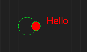
This adds the Exit symbol and an event-flow between them showing a minimum, legal diagram. To draw this you first select the Entry/Exit symbols adding them, secondly you select Event Flow and draw a line between the 2 red dots. The dots dissapear as the events are connected. An output must connect to an Input etc.

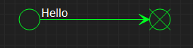
The next is the State symbol itself. As you select a state you can chose between a generic sub-diagram, block of C++ code or premade component. All state’s will have a list of input and output events that at start will be displayed as Red or Green dots. Red dots represent abstract events that must be connected, while green dots represent virtual events that you can chose not to implement. Virtial events can also be hidden (tagged as ignored).

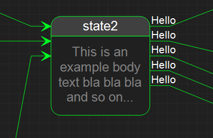
The dots will be replaced with lines and normal text as events are connected. The text “This is an example body..” will reflect the actual content – or by your choise a free text. The standard actually have a entry/exit notation – and I will need to do some adaptions on that.

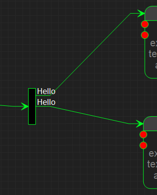
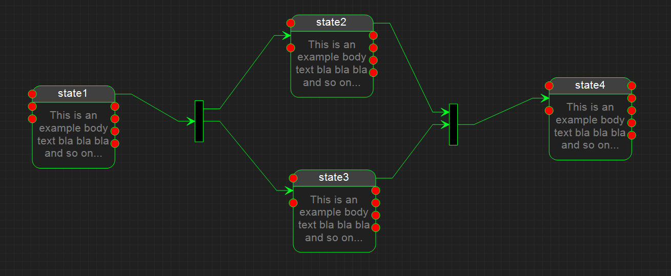
This is a Fork where an event is duplicated and sent in parallell to two different states.

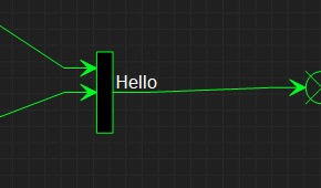
The opposite of a Fork is a Join that syncronize events.

As mentioned – this is an experiment, so I need to adapt as I go to develop the tool. The technique is not as mature as PLD and I am not sure about it’s actual worth, but I like the concept and want to see if this way of coding actually add value then done right and in combination with other techniques.

The tool itself needs a bit of work before its usable for anything and its an experiment as I complete the graphical editor that will be used for PLD as well.


UML Designer

Just showing a test diagram on the UML State Engine Designer I am making. It is stoll lots of work and details left, but progress is actually going fast the days I work on it. As for now this is just an experiment. A state engine can visualize some top level flow, but the details of the logic get hidden. My plan is however to let users chose between sub-state diagrams or code editors and see if that works out. It is regardless a cool tool even now.

The red dots are pre-defined events – input on left and output on right. Red means they need to be connected. As they are connected the red dot disapear and is replaced with the connection line. One trick on a diagram like this is to automate lines to avoid that users spend time making lines look nice.

Keep in mind that this is an automation tool that will generate source code, it is not a drawing tool. That said precentation of readable diagrams into doc is one of the objectives.

Interaction with source code and/or PLD is straight forward. PLD is excellent for visualizing logic and will handshake well wil State Diagrams.

Analogue Data Acquisition Hat

One of the big advantages with STM32 is that they have a range of MCU’s from the small M0 series to the more powerfully M7 series. Changing MCU to scale up/down is very easy. The MCU’s will have some differences in pin usage and register usage, but ST have been decently good at keeping their stuff as compatible as possible.

Pricing is another issue, buying through a distributor it is not that much difference between a M4 and M7.

The differences between these two are huge. H7 runs at 480Mhz, have 1Mb SRAM, 16 bit ADC channels etc. This is of no consequence if all you want to do is to blink a led. I have standardized on STM32F405 and that alone has far more power than I need for most parts.

STM32CubeIDE have also changed + H7 comes in a 100 pin package. The ADC channels combined with 1Mb SRAM and M7 opens for interesting data acquisition techniques so I have decided to try out the H7 on a Analogue Data Acquisition Hat. In fact I can use my existing nucleo to test out SW concepts, so I don’t need to start with HW in this case.

DDS Function generator

This has been on my list of things to do for a while and represent a few challenges. Chips like AD9851 contains a full DDS that interface to a MCU on one side and give 3.3V signals on the other side. I have yet to decide wherever  to use AD9851 or something else, butAD9851 is the candidate as we speak.

The block diagram above outline the functionality of the DDS. The first part a MCU  and AD9851 is straight forward. I have not used AD9851, but I have breakout boards + loads of reference schematics to work on. If nothing else I will make a Hat with 1 x 3.3V out channel. In many cases that is all that is needed and with my capability to stack up Hat’s we already talk about a very nice instrument.

The PSU is straight forward. I use 24 or 48V to create +/- 12 or 24V out as base. The amplifier is however far from straight forward.

First step is to offset the 3.3V signal, the second to amplify it and remember that we talk about signals up to 70Mhz. The Hat might get crowded, so it is possible that I need to split this onto 2 Hats and as such also accept that the amplifier only support 1Mhz or something.

I have dreaded this project a little because I only was on 2 layer designs, but as I now have moved to KiCAD and 4 layers or more is possible I want to give it a go. I think the first step is to make schematics for MCU and AD9851 as well as playing around with my breakout boards a little.

The primary usage for this is test equipment and it’s fun to make your own, but most important fun to have this as a component in my modular system.

KiCAD 3D Packages

I must admit that the realism in KiCAD’s 3D model is growing on me, it is great for precentations in here. Adding a 3D package was about selecting an associated 3D model file, so from now on I saved a copy of this footprint with the associated model in my own extension library.

Adding drill holes was easy – it actually is a component selection in the library, so all I needed to do was to select the correct one and set dimesions/position. On these drawings I had to switch off realistic mode on the backside to actually see drill hole areas properly.

One advice is that KiCAD actually crash from time to time. It crashed as I tried to remove the old via’s, but I opened the file in a text editor and removed the objects manually.

Target 3001 had a script option to make your own 3D packages. Basically you have the same in KiCAD since files look like scripts. But, the better way is to use some 3D design tool that can save in the correct format.

As for the 32xServo/IO – I could only find the SMD version of the 1.27 pich JST connectors (CAN port) and they are a bit wider. I am not sure about this choise, but I will try them out. I need to find or make angled pin-headers 3 row deep and 2 more packages. I would also like to tilt a few things 45 degrees and add text, but other than that I am done – I have basically made my first prosjekt in KiCAD.

I have to credit the community for all the available youtube videos on various subjects – without those this would have been a much harder learning curve. My next task is to start making the boards on 4 layers. We are actually setting up our own assembly factory a few miles away from my lab. That said, I am not sure how to deal with production yet – it is down to logistics and even if I can assemble low cost I still have to ship units out. The later cost to much from Norway, but that is a different story.


32xServo/IO Hat Rev 1.4 Annotated

2nd Draft of my new 32xServo/IO Hat rev 1.4. Added the leds and missing SPI resistors + reorganized connectors at bottom. I notice that I need to add a capacitor to assist D2 (TVS) on the bottom + I want to add 2 jumpers allowing left and/or right array to be connected to 5V as supply +++ but, I am in no hurry to order this. As mentioned before I still have not fully tested rev 1.0 and it is mostly cosmetic changes. But, this has an obvious change that I put all analogue capable channels at left and all PWM only at right + to more care to use as many HW timer channels as possible. In the end I managed to grab 25 Hardware timer signals, leaving only 7 for SW bit banging.

  1. CAN 120 Ohm terminal jumper.
  2. CAN Port.
  3. 16 x Anague capable Servo/IO channels.
  4. USB Port. Great for development and stand-alone operation from PC as well as downloading new firmware.
  5. Servo power Connector.
  6. Leds 1 Power Led and 2 MCU leds.
  7. 16 x PWM only channels.
  8.  8 x 4 channel 5V TVS to protect MCU ports.
  9. 4 x drill holes in Raspberry PI 2 position/size.
  10. SWD connector.
  11. Raspberry PI 2,3,4 Connector.
  12. Led for CAN port indication.


This block diagram show the actual channel per channel capacity and what MCU signal I used as base.

My challenge now is how to order a PCB? As mentioned before Norwegian import rules changes 1.Jan.2020, so I get slammed 20.- USD on a 10.- USD order. I need to find ways to avoid those handling fees, but it will take time before sellers abroad adjust and start declaring Norwegian MVA. If Elecrow declare MVA I would pay 2.5 USD for a 10.- USD order, if they don’t I end up paying 2.5 USD in VAT + 20.- USD in handling fee. One solution is that I wait and order many PCB’s together because the handling fee is the same. Doing this on PCB is doable, but on components it is close to impossible. The drawback is that samples will start costing 3-4 times if I can get them at all. Don’t worry, you will hear me whining about this for some time until I find a solution.

32xServo/IO Rev 1.4

First draft of 32xServo/IO Hat. Designed withh KiCAD this time, but still a 2 Layer design. I lack 3D packages for Power connector, USB port, JST CAN port and Q1 Crystal. The Q1 Crystal footprint was my first footprint design, but is was rather straight forward. Next I will have to try adding a 3D package. The 3D model uses “Raytracing” and option in KiCAD to make the board look more realistic. You can see the ordinary 3D model below and make up your own mine. A 3D model is a 3D model, it has a functional purpose so I must admit I prefer the one below because it is faster – much faster to work with. But, it is nice to have options.

And yes – leds are missing. In fact many of the changes I discussed before needs to be inserted in the next draft.

Changing footprint and 3D model on Target 3001 was done in a proprietary scrip language that had its sides. My main challenge was that it took time and you forgot the script language between every time you used it + it was not well documented. Making footprint in KiCAD was very visual and straight forward – time saving.

KiCAD – PCB Layout

One of many new features that was not available in Target 3001 is display of signal names on tracks and pads. I selected the wrong footprint for SWD, but as it is the same size as a 1.27 pitch header I did not think it matter before I noticed that it count the pin differently – wherever this bug is in schematics or selected footprint can be discussed. What is important is that KiCAD allow me to see it.

Another feature is the capability to drag entire sections of lines to make room for a new one- The level of semi-automation on KiCAD is really impressive. I am actually routing manually, but the automation allows me to move earlier content to make space and suggest alternative routes from where I am with such an ease that PCB routing is done in a fraction of the time I needed with Target 3001 – and I considered Target 3001 to be easy to work with.

This is still a 2-layer layout for now as I am learning KiCAD properly the only way it can be done – by using it and gaining experience. But, I have not used the backside much at all do to the routers capability to find or make paths. It will obviously take a few weeks before I truly master KiCAD and I will not spam this blog with details – I think most of you get the picture by now – KiCAD was something I should had started on years ago! That said – getting started with KiCAD is a bit heavy so you must set your mind and start digging in watching videos and try and fail. KiCAD has to be learned the hard way, but it is worth it.

As for suggestions on how to improve KiCAD – don’t worry, I have plenty. The first I would start with is to merge the two screens that (1) allow you to watch footprint and (2) allow you to select footprint because the first let you see the footprint while the second don’t – luckily I van have both open at the same time because it’s a bit hard not seeing the footprint you select. But, again – you don’t want to hear about how I had to do this earlier + yes it’s a button to open a 3rd window where you can see the selected footprint 🙂

Looking at the backside pic above I notice how little I have used the backside – which is good since we are on 2-layer, but I also notice that I still have to learn how to deal with drill holes yet. One thing at the time.

The last think I wanted to show you is the semi-auto router. As you select two points on the PCB KiCAD will attempt to autoroute that lane. In this case I was more impressed that it actually found a path – I will not be using this one, but many times I do and end up routing much more single layer than before. I can now draw part of the lane manually by clicking on connection points and the auto-router will take it from there. And you can always use the drag function to optimize path afterwards as well. This is a big time-saver compared to how my previous tool worked. I assume it exist a full auto-router as well, but I have not tried that one yet.

Thanks for reading my early morning ranting…

Ordering new PCB’s

It is soon 1.jan.2020 and Norwegian import rules changes, meaning I basically get MVA and a 20.-USD handling fee on every package unless I get the foreign company to declare MVA. It will be a pain and take some time before this happens. Ordering parts from Asia will be close to impossible unless you order big quantities. It feels like my country are reverting back to the stone age…

2-Screens in use w/KiCAD

This is a screen-shot of my two screens. I have PCB router on left and schematics on right. As I work on PCB the schematics will show the associated part – neat little detail. KiCAD is actually multiple applications so its perfect to take full advantage of multiple screens as you work. I have routed 60% of the new board in about an hour – most times just playing around – KiCAD is so quick to route that it is amazing. The auto-router is also good at finding track options allowing me to stay as much as possible on the same layer + it’s a real pleasure to use via’s.