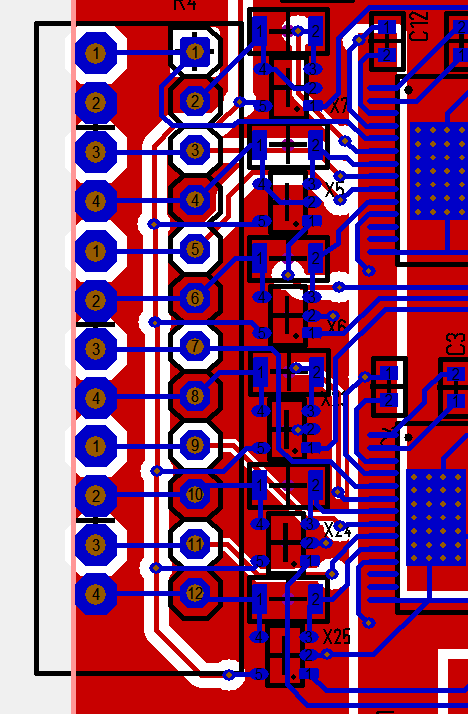
Left side of the 3-Phase/Stepper/PWM Hat done. This is the hardest bit, but it went much easier this time because the previous attempts gave some hints and lessons learned. I am far from finished, but it is not hopeless. My main concern is the ground-plane getting to fragmented and unable to support the currents – but, I am not out of tricks yet.
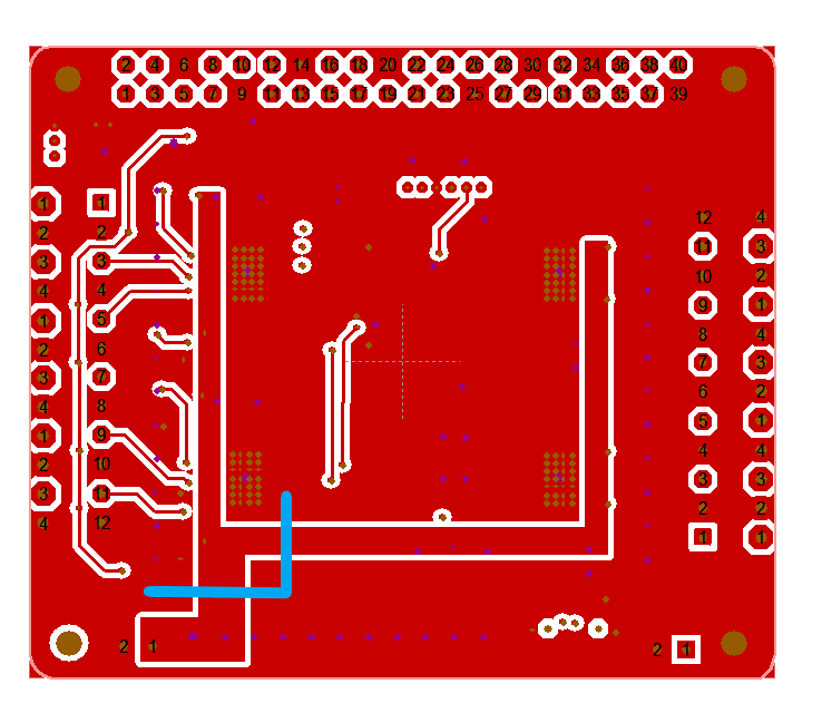
This picture show the back-side and the ground input is actually the “2” in the left, bottom corner while DRV8313 are on the inside of that thick 36V power lane. While Ground is connected you can see that it is thin on some places due to the density on the left side. it will be equally dense on the right side, so what I am considering is to add a bridge on top lane (illustrated in light blue) to ensure that I have a direct path that will support the currents I need.
I must admit that doing PCB routing is a bit like a puzle. You need to like these mind games if your going to be good at this. I know many electronic engineers who seldom do PCB routing – only schematics.
I have suffered “Crash O’ Mighty” on this Board a lot. I use a free version of a Target 3001 EDA based on Java and well – it does crash a lot. I am also more and more feeling the pain and limitation of 2-layer designs, but I will need some time to get started with KiKad.
What worries me a little is the signal integrity of the current sensor signals. But, it is nothing I can do about that. The issue is that the ADC signals need to pass strong PWM signals, so that current on one PWM might give a false signature on a 2nd PWM’s current sensor. I do however have the option to filter and compensate for this in software, so lets see. I do expect noise on these signals regardless.