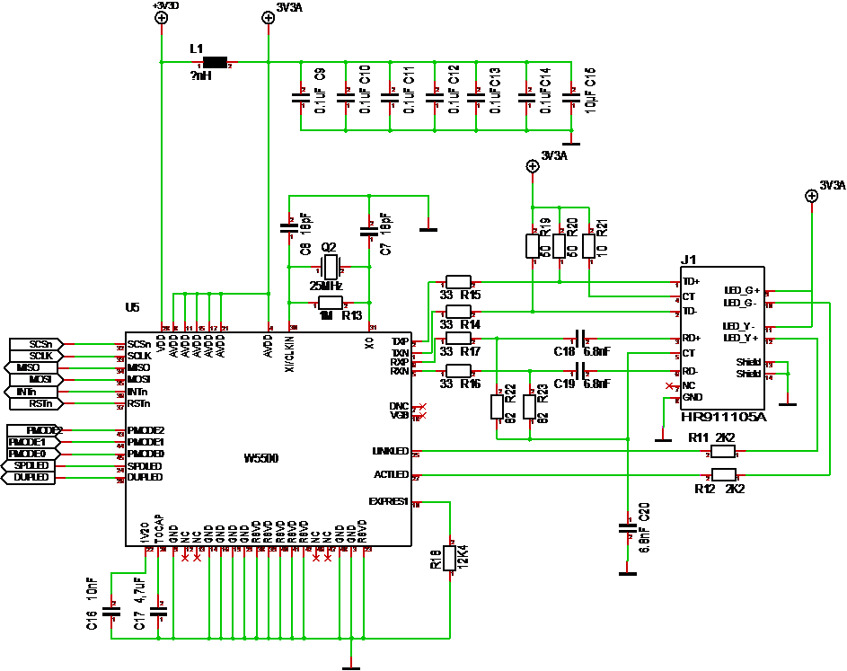
Updated the W5500 Ethernet schematics. C9 to C15 present a challenge in PCB routing since I am using 0805 packages. They are supposed to be attached close to each AVDD pin which is a challenge. Also I added the L1 ferrite bead to stop 100Mhz signals from crossing over.
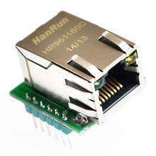
But, I am still thinking that the 8.- USD breakout (below) is a tempting simplification. Particulary since the footprint will be smaller with this. I am also thinking that these breakout boards will even drop in price later.