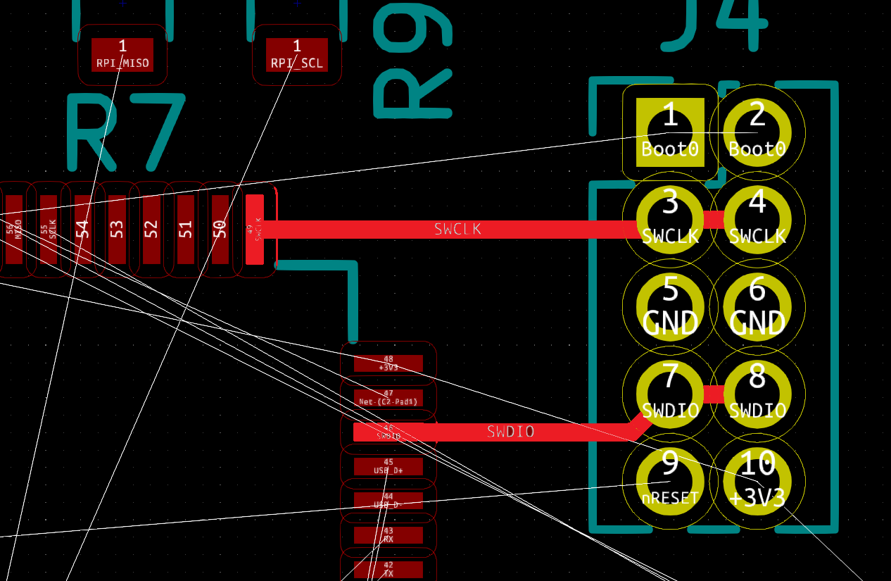
J4 at right is the SWD connector. This can be reduced to 3 pins (SWCLK, SWDIO and GND), but it is wise to include Boot0, nRESET and 3.3V. I have painted SWCLK and SWDIO lanes in light red – those are the important ones that needs to be kept as short as possible. The only reason I use a 2×5 pin connector here is because they are easily available and give a stable connection base as I add a 1.27 pitch to 2.54 pitch adapter on top. It also gives the advantage that I actually can program the boards using a male adapter and just putting it down the holes. I recommend a proper connector if you work with the board, but this is a neat production trick to avoid mounting connectors on all boards.
This is my latest SWD format that I know apply on all boards, but I have so far used the same adapter board on everything and it have worked very well. I usually have a few ST-Link/v2 with adapters and it’s very easy to connect to board – which is how it should be.
I will however make a new adapter targeting boards inside a stack. I can manage with my existing ones, but I need to dissassemble the stack to mount/remove adapters. I want a new adapter where the PCB take me outside the board so I can mount/remove SWD’s while they are part of a stack.