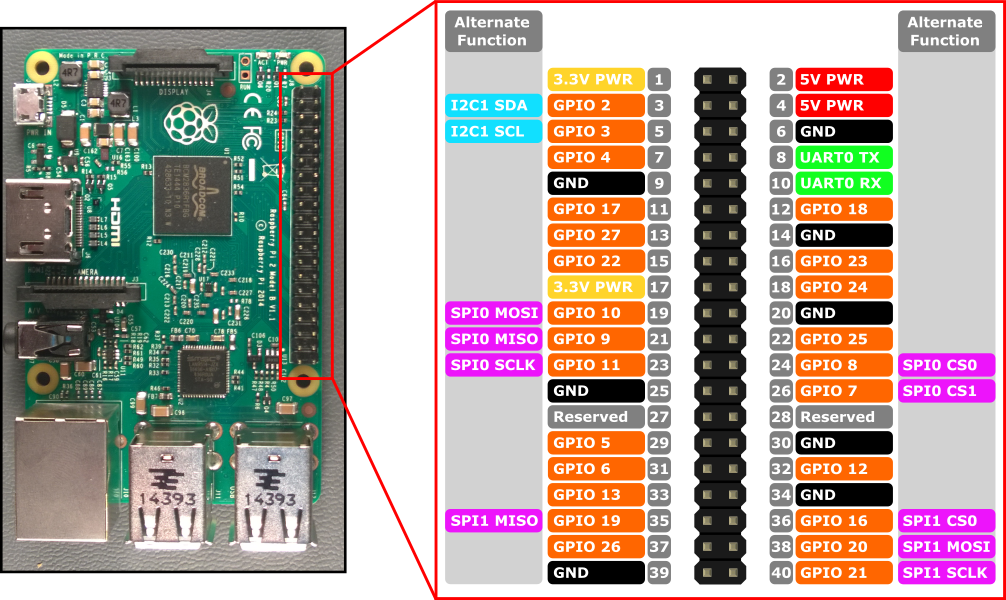
 I was in the middle of planning a 8 pin bit-bang bus as my attention was drawn to STM32G070KB that cost 0.7 USD, comes in a LQFP32 package and contains: 2 x 1Mbps I2C, 2 x 32Mbps SPI, 4 x 6Mbps USARTS, 128Kb Flash, 32KbSRAM, running at 64Mhz and 7 DMA channels. Looking at the RPI pinout (above) this becomes very interesting.
So – what if I drop my bit-bang plans and use the two SPI’s for data transfer on the bus while I use a 6Mbps USART for communication with STM32 – basically dropping SPI between F405 and RPI bus? A 6Mbps full duplex UART backed by 2 x 32Mbps SPI’s is a lot of bandwidth.
Funny how things evolve – I started this by wanting to add an on/off switch to my boards – and we still have that as well – I also have several ADC’s and GPIO pins available on G070 so I have options in solving the tricky start up scheme. But, I need to draw sequence diagrams for the various situations to convince myself I have solved this.
I plan to use a I2C for a EEPROM storage. FRAM would be better, but it also cost more – lets see. A 32 Kb EEPROM also provide config storage space for F405 – so its far from wasted.
Moving on – I have space on top to add these components. My main concern is interference between the two MCU’s so this will force me up to 4 layers and components on both sides. I need ground planes between the MCU’s unless I manage to mount them on same side – but it is getting crowdy on some boards. SWD can be connected on RPI bus so we can program Device Bus. I am starting to like this concept 🙂