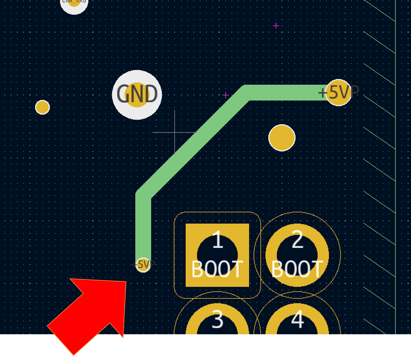
I was warned ny JLCPCB that my boards had some strange pad’s – looking at KiCAD I notice the issue above. These via’s are set to have Pad on connected layers only and KiCAD screws up. If I click on the via it correct itslef. Will be interested to see if this board works at all. JLCPCB offered to redo them, but I will just leave it for now. I will test if they connect as they are supposed to, if not I will redo them. The Ethernet module and motherboard should be ok – the PWM3 and PowerServo2 will have this issue.