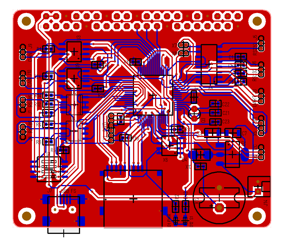
Routing a PCB is actually a bit of work, but I enjoy doing it a few hours early morning and late evening. It is easy to pick up and then just leave, and over 1-2 weeks I usually get a design done like this. It is always a special feeling to suddenly find that you have no more green lines and can start the checks. I am actually not fully finished here as I need to modify the Micro SD package + I would also like to replace the 1.27 pitch headers with connectors 3D because I need to adjust their distance to the edge. I also need to check my alternatives on footprint for the Super capacitor and battery. I ditched the GPIO header because I have only 3 pins left and will see if I can route them out as leds. But, this looks good!
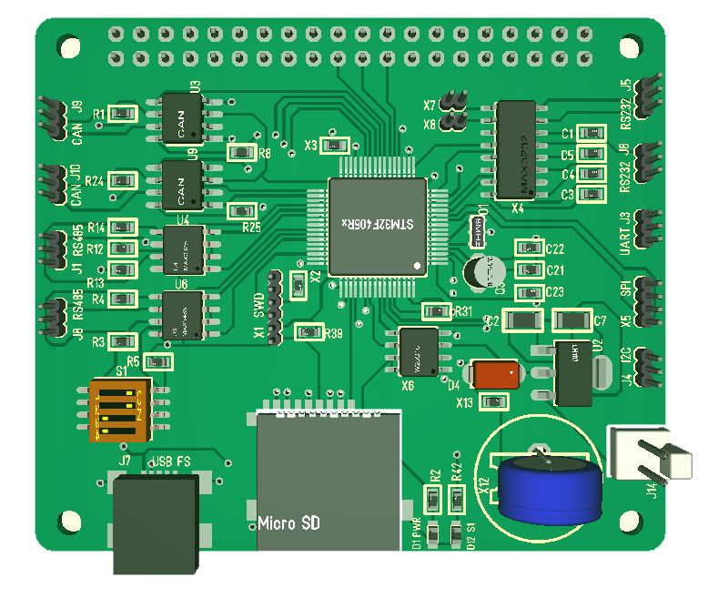
This is the PCB the way I usually see it in the EDA without the ground plane.

This is the PCB the way I usually see it in the EDA without the ground plane.

I use ground pane for connections to ground to avoid ground loops, but the EDA have an error that it does not warn me about isolated icelands. So I remove components and top layer and copy it to MS Pain using fill. That will indicate what icelands that are left. In this case it was several that I managed to change so they got connected. The small ones left in the middle has no connections so they can just be left.
I will do the last check later today and off we go – next time you see this will be the actual PCB in 6-8 weeks. I had a bit of challenge finding a name on this, but decided to call it “X Hub”.