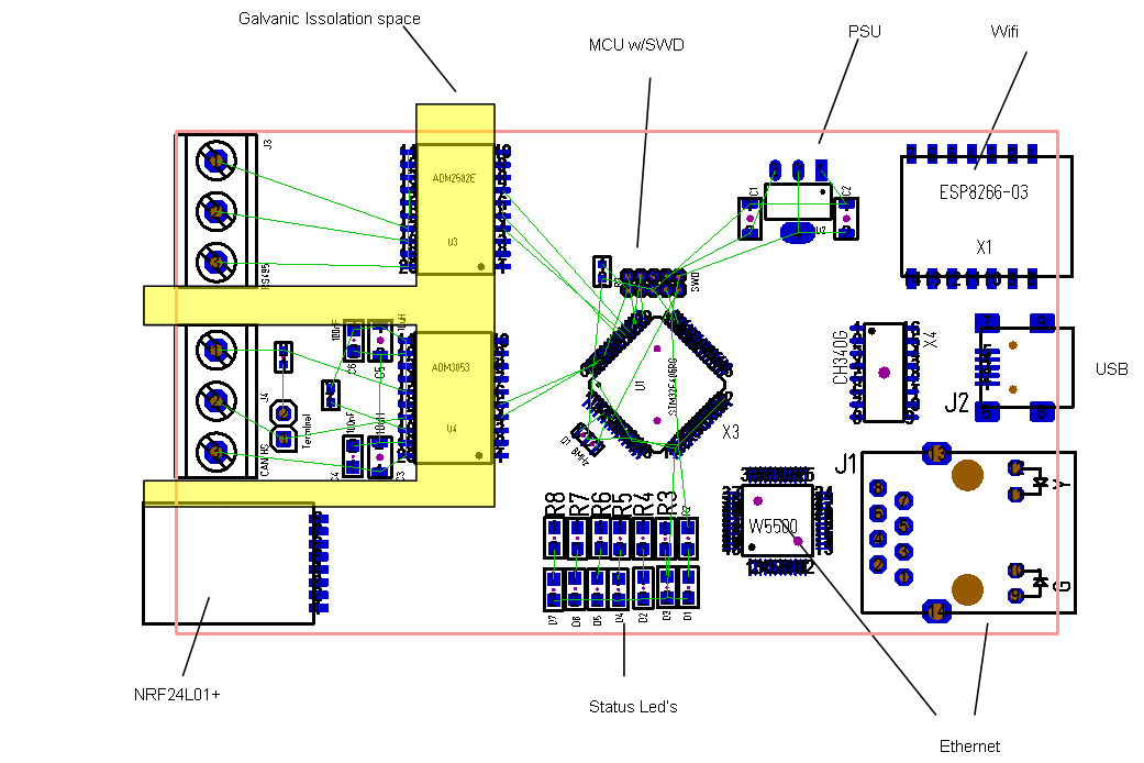
This is an early draft with only the main components mounted. The schematics are not even close to done yet. I like to place main components straight away to get a look & feel and in many cases I adapt schematics to physical layout. I know some prefer to complete schematics before they start PCB layout, but with modern tools I find it easier to just get the packages and dump them on a PCB. The larger chips often need to be rotated for optimal routing and sometimes you can change components or select a different SPI/UART etc based on what is most optimal.
I have several issues already. The areas at left with the yellow marked isolation space is fine. I have plenty of routing space in that area. The area around W5500 is however tight. An obvious solution would be to swap Wifi and Wired Ethernet. I don’t want to move the led’s up because they will end up under the SWD adapter, but moving W5500 up should work.
I have used ESP-03 simply because I had a pre-made package, but I am thinking of replacing it with ESP-12E. The later is a little larger, but have the same form with legs on the side that will hold the breakout board in place. The NRF breakout have an issue as all legs are on one side. This will make it weak as the other end will tilt up and down and vibration might break it loose. I have seen different solutions for NRF24L01+ so will look into that. The USB is placed in the middle away from the edges because it is held with those 4 large pad’s. These are GND and need extra support to provide mechanical strength to hold the USB as we plug in and out. As mentioned in an earlier post I had issues with this on a different board.
I hope to have the first draft of this ready to order PCB’s tomorrow.