PLC – 3xPWM Finally Done

86 components on 25 x 45 mm – it don’t look like much in 3D, but it was actually quite hard to route even on 4 layers.

  • MCU STM32G491RE
  • DRV8313 for 3 x PWM
  • 4 x Current Sensors
  • 1 x DC Input Sensor
  • 1 x CAN-FD Tranceiver (IPC)
  • 1 x RS485 Tranceiver (IPC)
  • 32Kb FRAM
  • SW controlled terminators
  • 8 – 24V support
  • 300uF capacitance on 24V on-board.

Some of you will recall that I made a similar module before (below). This was 20 x 50mm and 2 layers. It has a 60V DC/DC that worked with a tweak and hall sensors that I never tested – but it was components on one side only. The motor driver worked well – it was CAN here as well. I never used F303, I just used F103 instead. But, it is a 48 pin version of the MCU, No FRAM and no current sensors on this – and it lack capacitanse on-board.  This old board was tested with 50ich Volt, but  I  realized later that  some  of the  capacitors  did  not  hold the speck  – fake  Chinese  crap.  The new  board  will  not  be using components  bought  on AliExpress  – lesson  learned!

Having done an Ethernet Module and a PWM module I want to just get those assembled and evaluate the format as I go. Looking at the module above you can see that is no space for 2 extra SOP8 circuits and 4 current shuts – the circuit above is 40 components, while the new one is 86 components – I literally have no free space on the new one.


PLC – 3 x PWM Module

Showing 3D of the 3 x PWM Module. I had to reduce Voltage to 24V due to capacitors, but 12V or 24V should be ok. I added a 2-pin header for PWM Voltage and a capacitor bank as well as the 4 current sensors. The TSOP28 has a PAD so the middle of the top layer needs to stay clean – I will look into getting 48V supported, but 24V is ok for this little module.


PLC – 4 Module Motherboard

This is the 3D from a 4 module motherboard. I originally planned to use standad 90mm wide boxes, meaning that the motherboard probably needed to be 86 – 88mm wide, but this draft is 91mm wide. It means I will have issues using standard 90mm low cost wide boxes, but 2,5 mm is a lot to cut on each board. The reason for the extra mm is because the motherboard need to leave ca 1 mm between boards otherwise it would be to tight. Board cuts are not that clean or accurate ans 1 mm gap leaves plenty of space for inaccurate fits.

Back to the box issue I am tempted to make my own custom boxes using a 3D printer. I also need some custom cover on the modules and that might cause me to leave extra space for per module, but that is for later. I like my 45 x 25 mm module design, so I hesitate to change it. The issue is that it is easy to remember and if I continue to shrink the board it will leave the format useless. This is actually a very small board as is,

I like the flat-packed, modular design because this allows me to assemble modular systems that is easy to fit on any equipment. The 3D module below show 4 x Ethernet modules mounted since that is the only module I have yet. I have not added headers on the motherboard, but distance between motherboard and module is ca correct. One nice detail here is that adding electronic components on the bottom will shelter them a bit as well. The total width will grow to ca 100mm if I add a box per module. In that case I will have a bottom box for motherboard and a separate top box for each module + dummy for unused slots. That will add 4 mm on each board – 2mm on each side – so the modules would be 49 x 29 on the outside and 100mm wide in total. I need to work on the mechanical design details, but I think this will work out fine. The ethernet module have some extra height due to RJ45 module and it’s headers.

Just adding a differnt view – removed the modules at right and moved in the template module 3D to give a better idea of how a real system might look.

A minor detail here is that I have started to export picture more directly from KiCAD – something that saves me time.

BSA – Using a PLC PWM Module

Using a PLC module (or any component) in BSA is straight forward – you simply declare an UML State symbol with the input/output events you need and set this as external with the selected interface protocol and addressing scheme. The protocol can be anything because BSA is after all just a visual specification, so the magic happens in the code generator. If you use a proprietary protocol you will need to implement that and interface it to the selected platform SDK.

Drawing it like above is physically correct as the message needs to be sent from a top-side (or control unit) to an Ethernet module that forward the message to the PWM using CAN (or RS485), but these are details that we can deal with in config – so I want to see the PWM module only as shown below. How “StartPWM” get to the correct PWM Module is something I deal with in configuration.


You can hard-code physical addresses in an easyIPC network, but a better way is to declare that you have a PWM node with capabilities and ignore the details of how we get the message transported. As you actually configure you system it will look for a PWM module in the network and let you chose which PWM module to use for this purpose. This is also how you replace a PWM module should one break.

I will return to this later as I start using my own system!


PLC – G491RE Template

I will be using a few MCU’s to create PLC Modules, so it makes sence to create a template – starting project for each MCU. The most obvious is STM32G491RE. This template contains MCU, CAN, RS485, Crystal, SWD, Leds, FRAM and PSU condenced as tight as possible towards one side.

The template might change, but the idea is to get a flying start on new modules. As for FRAM and RS485 – if I don’t use them it cost me nothing to not assemble them!

PLC – PWM/Motor Module

DRV8313 is an excellent driver circuit containing 3 separate half h-bridges that can be used as separate PWM drivers, a DC Motor driver or 3-phase motor driver. Delivering 3.5A max in peak and supporting upt to 60V it is excellent for 12V, 24V or 48V systems. I have made a small motor driver on this before and I only need a few passive components connected to the operational Amplifiers in STM32G491 to create low side current sensors. This will be an excelent PLC module and small motor driver.

The drawback with low-side current sensors are that it is difficult to measure individual currents simply because you will not use the low side on solenoid type connections, so high side current sensing is better, but this require additional circuits that drive cost/complexity. So what I will do is to use four current sensors – the forth measure total current on the PWM- (Ground) channels, while the three others measure motor currents. I have 4 operational amplifiers in STM32G491 so this should work fine.

A 6P 2.54 pitch connector fit exactly on the 17mm available on a 25x45mm module, and this allows me to offer 3 PWM+ and 3 PWM- (GND through shunt) connections – for 3 separate signals you use all 6 and I measure current using the 4th sensor, while for a motor you use 2 or 3 PWM’s and I measure current on low side. It is a few issues I need to consider, but this sounds like a great module that will be fun to use.

CAN (or RS485) is great here because I can make this PCB purple or even pay for multiple colors and hang them with LED strings directly on the chirstmas tree. Fun to come 🙂

PLC – Module Mechanical Design

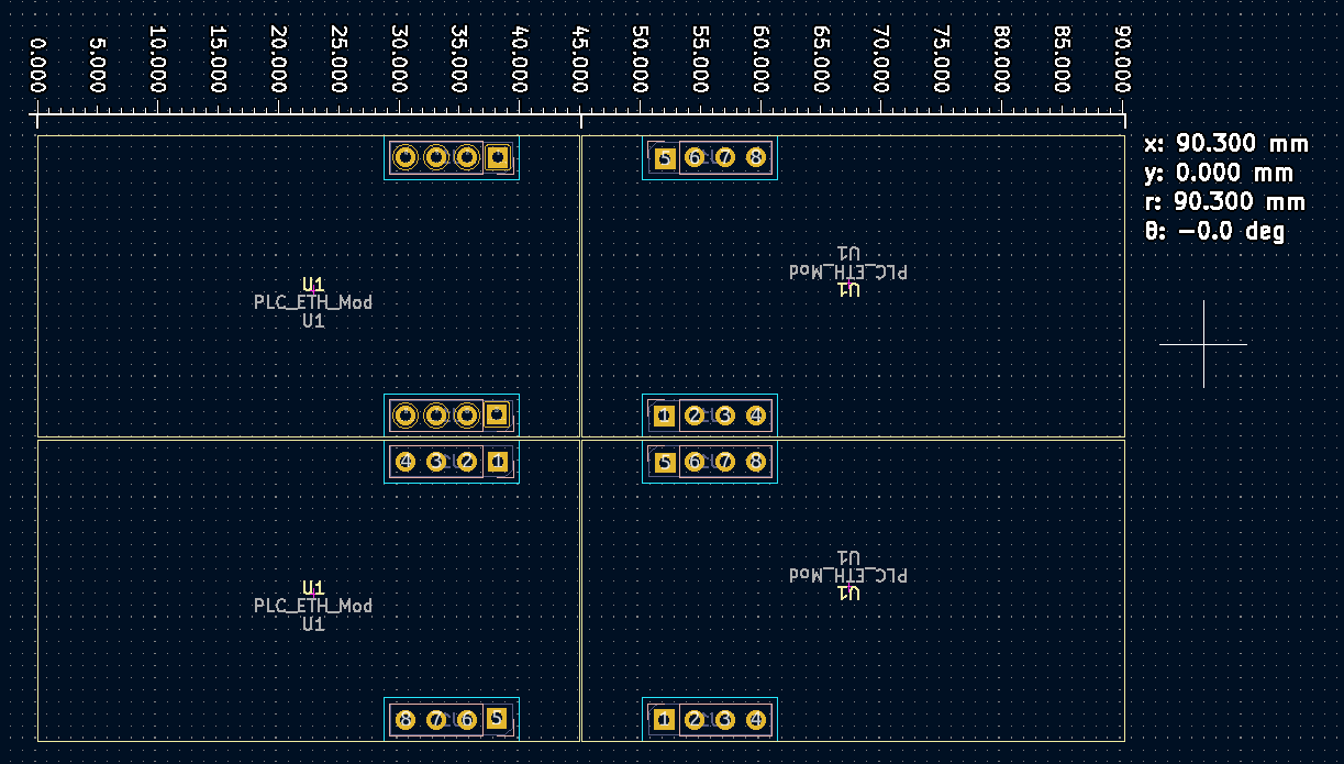
Before I order any of the PCB’s I also need to consider adjusting the size of the modules. I have ordered several standard project boxes that I will consider using, but I lack exact mechanical dimensions on them. And I have to figure out the mounting holes on the motherboard to the project boxes. The boxes I ordered are 90 mm width – hence the 45mm width per module. But, I probably need to reduce module width to 44 mm because 90 mm was outside the box + I need 0.x mm free space between modules as I mount them. The 25mm height was initially decided based on two criterias (1) I want the minimum module as small as possible, (2) I have ordered small project boxes that are 25x25mm size for two boards to go back to back. But, height is not so critical as width.

I have not adjusted this yet because without exact drilling holes and dimensions on the boxes I will need to redo this anyway. I also expect that I will need three PCB revisions – planing for less is just nonsence IMO. So, I will just order this modul “as is” and face the required adjustments later. Ordering PCB’s will cost me ca 20.- USD so it is more important to get going on testing so I get the prototype up running.

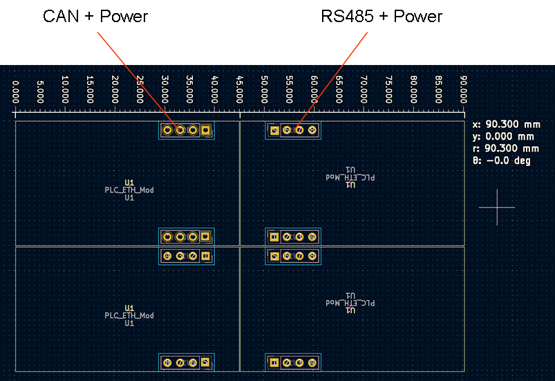
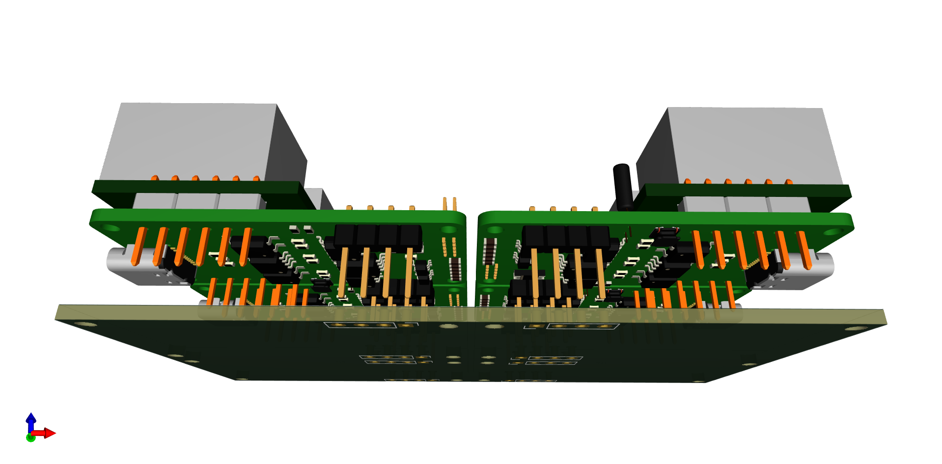
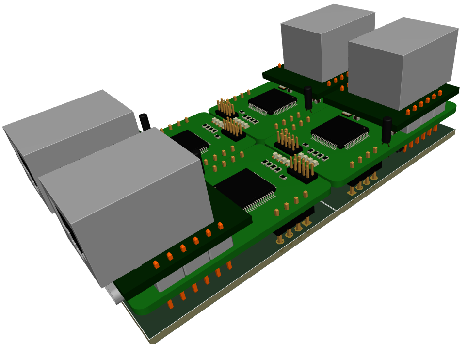
Notice that facing left I have CAN+Power on the top header and RS485 + Power on the bottom header, and facing right this is switched around. You can mount the module in any position and it will just work. I need to wak though the start-up sequence in SW and verify that I have what I need to make this work, but I think so.

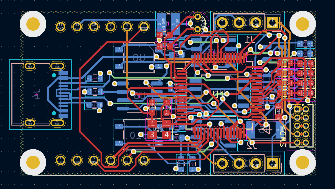
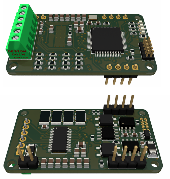
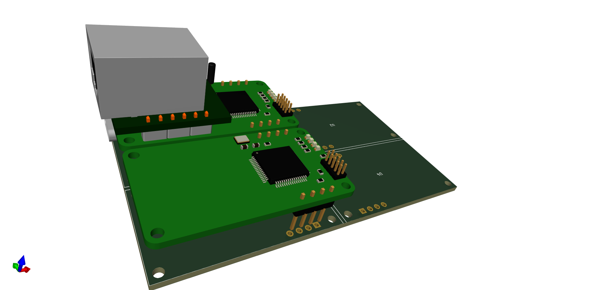
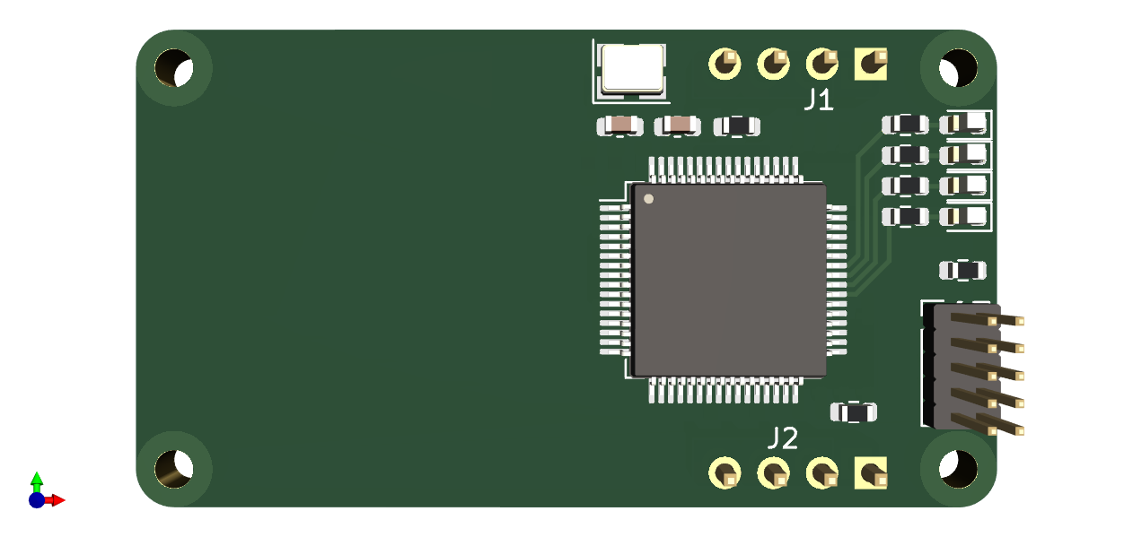
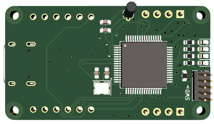
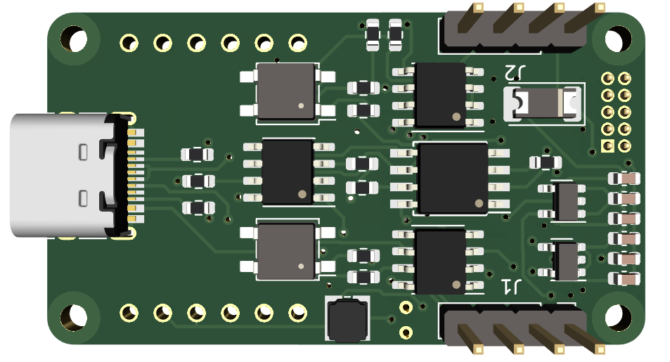
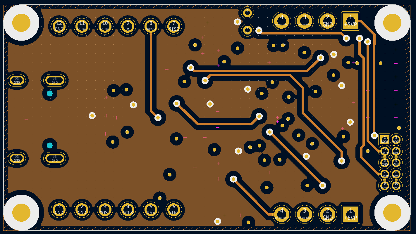
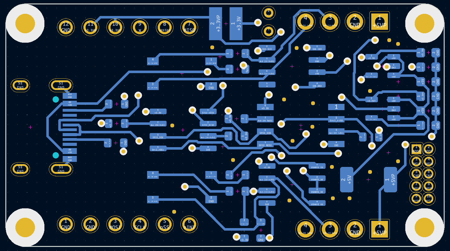
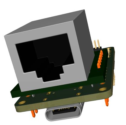
Looking at my Ethernet module you can see that it is easy to adjust 1 mm at the Width on left, but it is far more difficult to do the same on Height. I basically have to re-route the entire board Because I have 0,5mm space between the SOP8 components that I need to adjust in. And I need to use more of the backside in Width because routing and number of via’s are getting dense. The two headers, two resistors and 32Khz crystal must move in. If I need 2 mm then I can’t do it + I will struggle to get this module into 25×25 anyway because of the size of the J45.

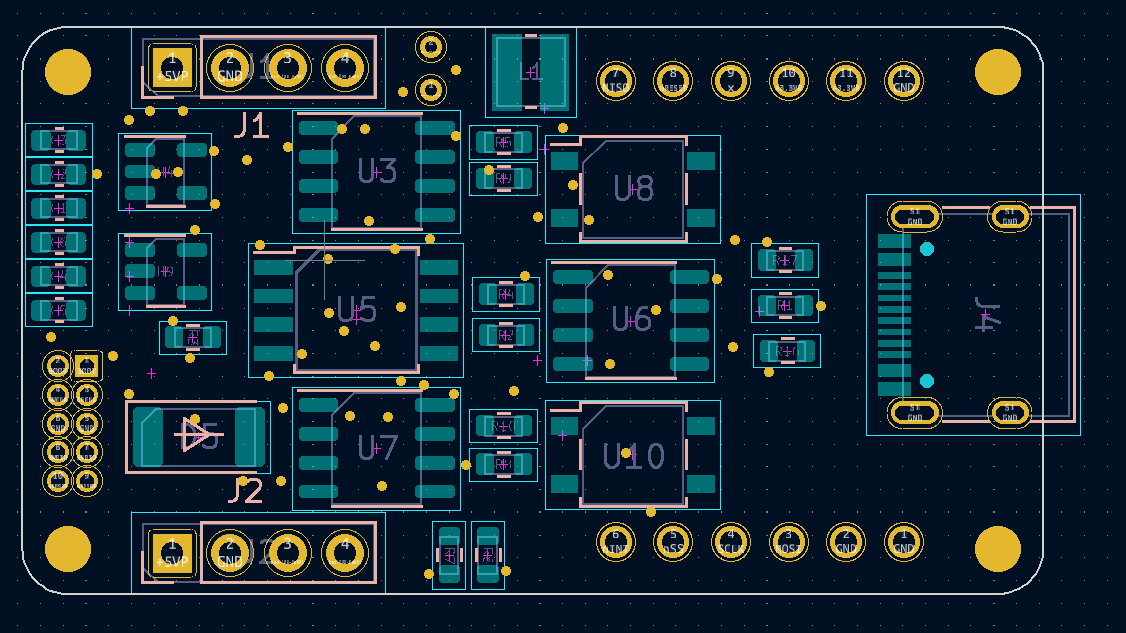
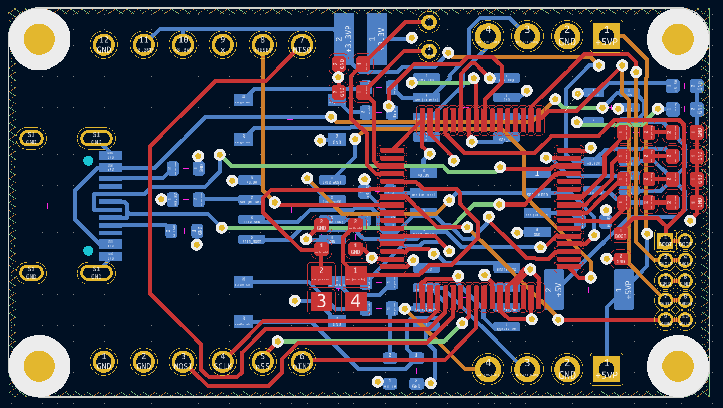
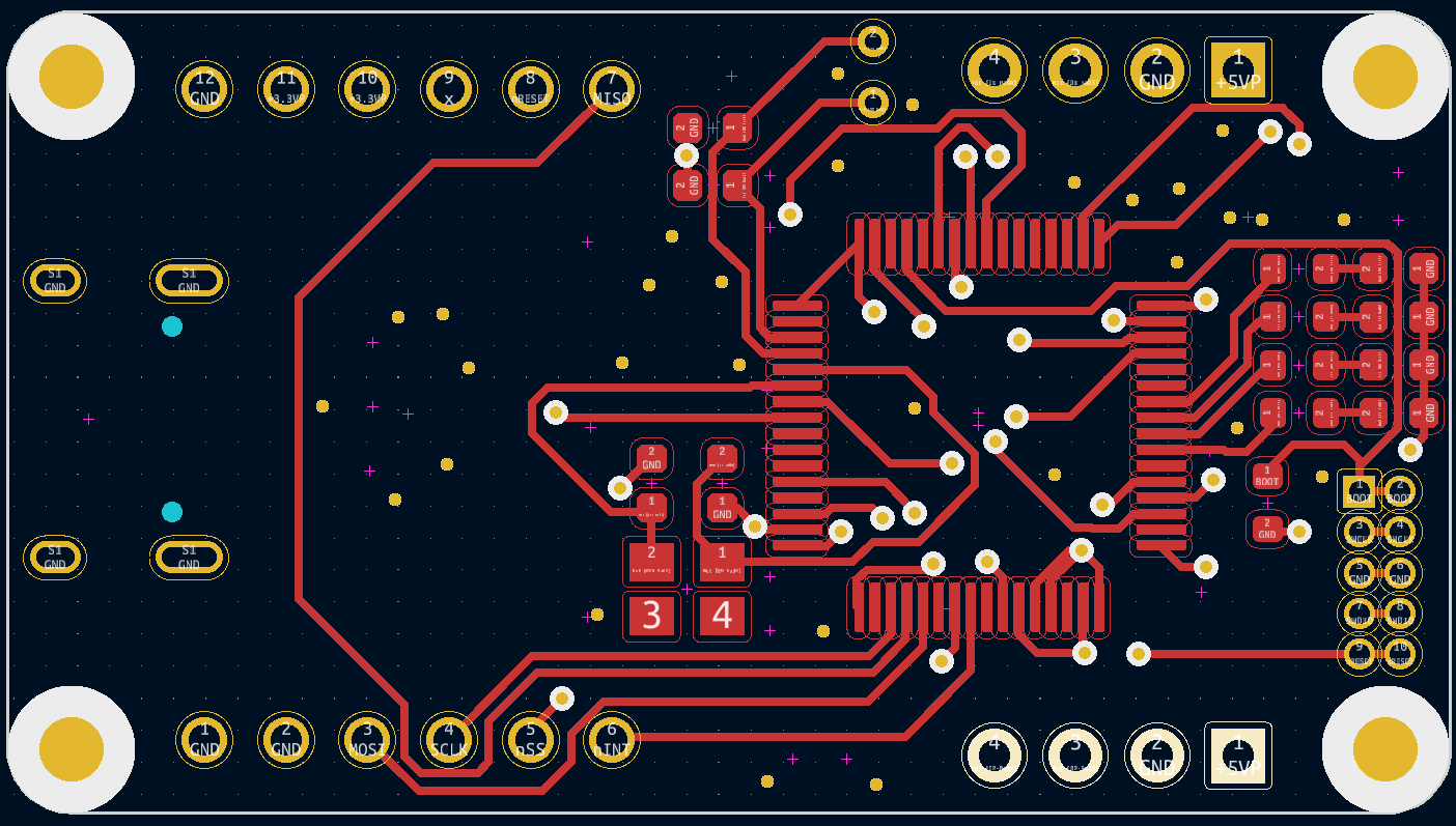
You see the issue more clearly on the back assembly view. What I can do is to swap U3,U5 and U7 with U8,U6 and U10 and mount them tighter as well as using more of the space towards J4, but that means starting from scratch on routing :(. TBH I should have considered these mechanical issues before I routed the first module, but I did not believe I would finish it this easy + I was not sure about what I could squeze in. You sometimes get fooled by how much space that passive components and tracks take up. All in all I am very happy with my first attempt on 4-layer PCB. In this case I also have 2 x 2.54 pitch headers and I often experience that they take more space than you expect.

Routing PCB’s I have discovered that what works best for me is to just get started and see how it goes – if I fail I restart – this is far faster than sitting around considering dit and dat for ages – far more fun as well :). Routing for me is like a little mind-puzle I can work on every morning and in spare moments – it is actually relaxing since I have no time pressure.

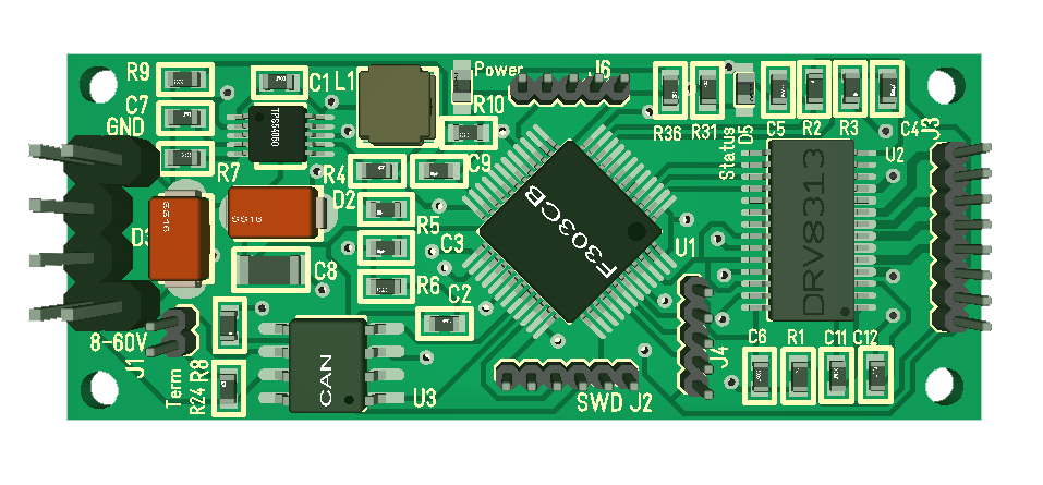
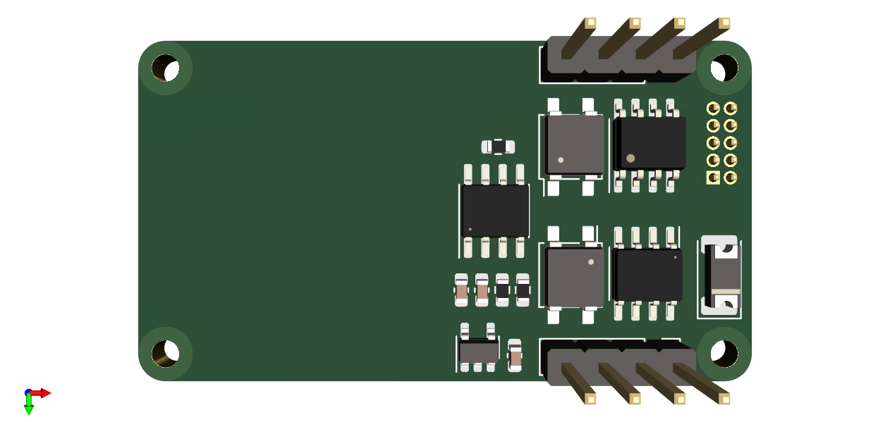
I did consider swapping out my SWD connector with 1×5 pin or a PCB/Cable solution. That cable costed ca 70.- USD so I ditched it and the reason I use 2×5 pin hole though has to do with stability. The only challenge I have with this format is that it sometimes is hard to see what direction to mount the SWD.

Don’t worry – this is the last you will hear about this Module for a few weeks – thanks for reading!


PLC – Motherboard

The next module I want to make is the motherboard(s). I want to start with a 2, 4 and 8 module Motherboard. An early demo of a 4-module board is shown above. In this case I have mounted 4 x Ethernet modules – an advanced system will usually have two Ethernets for redundancy, but you can actually mount your own Switch or Router this way.

Somehow the drill holes dissapeared as I made step files of the Ethernet module, but you get the idea.

Wise of experience I also want to wait a bit before I order more modules. Mounting a motherboard and a few Ethernet modules will most likely cause some changes to the design based on what I experience. I have a list of ca 30 modules I will like to start working on.

PLC – Ethernet Modul Finished

Fisished routing. One days work – first attempt on 4-layer design. I must admit KiCAD did most of the job.

Components top without Ethetnet modul.

Components bottom layer

All layers. I decided to use Ground and Power as the middle layers.

I don’t add ground layer on top or bottom since this will be hand-soldiered. Will use 1-2 days to check my work before I order PCB’s.


PLC – Ethernet Front

This prototype have a Wiznet breakout on top and a USB-C on bottom in front. The Wiznet breakout cover the M2 screw holes, so mouting these will be a little tricky, but doable. I will consider pushing the breakout a bit in-I need to alig  RJ45  and  USB-C infront  anyway and that will help.