Rock PI 4 b

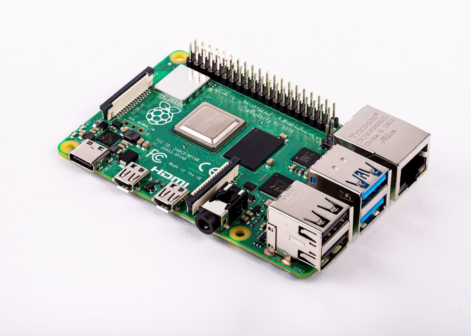
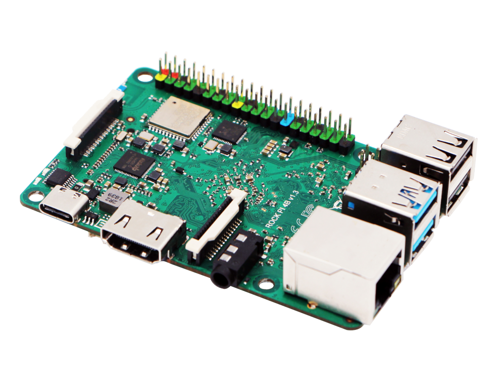
I accidentally came across “Rock PI 4 b” and first believed it was about Raspberry PI 4 as I realized this is a board based on Rockchip RK3399. It is very similar to Raspberry PI 4, but contain some very interesting differences. Of most interest for me is that the form factor and GPIO pin layout is compatible, meaning I can use my Hat’s on this directly. Lets outline some of the differences.


Rock PI 4 b Rasberry PI 4 b
CPU RK3399 BCM2711
Cores 6 Cores

2 x A72 @ 1.8Ghz

4 x A53 @ 1.4Ghz

4 Cores

4 x A72 @1.5 Ghz


GPU Mali T860;P4 VideoCore VI 3D

500Mhz 32 bit

RAM 2,4Gb 1,2,4 or 4Gb
Micro-SD Yes (128GB) Yes
USB 2 x USB3

2 x USB2

2 x USB3

2 x USB2

USB OTG Switch Yes No
RTC Yes No
eMMC Socket Yes up to 128GB No
PCIE M.2 socket Yes Support up to 2TB SSD No
Ethernet Gigabit Gigabit
Wifi Yes Yes
Bluetooth Yes Yes
Sound ? 4-pole stereo
Camera Port Yes Yes
Display Port Yes Yes
HDMI 1 x Standard HDMI 2 x micro-HDMI

2 x 4Kp60

GPIO 40 pin RPI standard 40 pin RPI standard
PSU USB-C 5V USB-C 5V
PoE Possible Possible
Price 67$  (4Gb) 55$ (4Gb)

The eMMC interest me as it allows me to boot from Flash making this an interesting option for more commercial solutions. Other than that I must admit that 2 x HDMI etc only is of interest if you replace your desktop PC.


Raspberry Pi 4

  • Quad core 64 bit Cortex A72 1.5 Ghz
  • 2 x 4K HDMI ports
  • USB 3
  • Gigabit Ethernet
  • Up to 4GB RAM
  • and more

Priced at 35$ for 1GB and 55$ for 4Gb this starts to look like a serious challenge for more classic desktop computers. I tried to buy one, but getting the “sold-out” from all shops. Read more at  https://www.raspberrypi.org/blog/raspberry-pi-4-on-sale-now-from-35/

Well done Raspberry PI

STCubeIDE Review

ST recently acquired Atollic TrueStudio and merget it with CubeMX into STCubeIDE. Having searched for a proper IDE to use I must admit this one actually do the job nicely.

To start a project you use CobeMX now integrated into the IDE, make your selection and as soon as you switch to code it is generated for you. It was a few tweaks to get C++ going properly, but navigator is 1:1 with file system and I actually see some benefits of using this compared to alternatives.

And best of all – it is free for STM32. Well done ST!

3D Sensor Hat – Block Diagram

First attempt on block diagram for the 3D Sensor Hat. The main components are FXOS8700 (Accelerometer and Magnetometer), FXAS21002 (Gyroscope), NEO 6/7/8 (GPS) and BME280 (Temperature, Humidity and Pressure). I am also attempting a TFT connection here, but this is secondary and can be ditched if needed. The rest is classic – Raspberry PI/SPI on backbone, CAN as secondary control bus, USB/SWD and STM32F405RG to drive it all.

Sensor Hat Finished

Final 3D of the Sensor Hat. The most noticeable here is that I start using the 2×5 pin SWD header. The rest is as described before.

  • MCU STM32F405RG
  • 1 x High Speed SPI for backbone
  • Raspberry PI Hat format
  • 1 x CAN for control bus.
  • 8 x 2 x Analogue/Digital IO Signals.
  • 3 x I2C ports
  • 3 x SPI ports
  • 1 x Power port
  • 1 x USB port
  • RTC w/Battery
  • SPI Flash

STCubeIDE

ST have lately purchased True Studio, so it was not a big surprice to see that True Studio now is merged with CubeMX. I am not a big fan of Eclipse based IDE’s, but this one is great for getting you project off ground fast. CubeMX saves you a few hours as you start the project, but I tend to re-organize my projects and move to a more professional editor/environment. I have been using Code::Blocks, but I actually want to set up Visual Studio Code. That said STCubeIDE is a nice alternative and they willhopefully mature the product out of Eclipse limitations. The concept is that you have CubeMX on one tab and as soon as you switch to C/C++ you auto-generate code. This IDE fueled by CubeMX is still a great starting point for checking hardware and getting your project off ground. Only be aware to follow ST rules as you add your own code or it will be wiped out.

New SWD Adapter


First draft of a new SWD adapter designed to be installed/removed while the Hat is inside the stack. SWD on this will work even if you miss a row while connecting because Reset is pushed to 3.3V and all other signals are duplicated on both rows.I will make another using ST-Link V2 connector directly. Currently I use 10cm wires between the USB adapter and this adapter card. Could be interesting to mount it directly, thought I am not convinced that will work well while the Hat is in a stack. Let’s see.

Sensor Hat – Mockup 3

Just added the package for CR1220. The actual package look at bit different, but this has the correct footprint and size. This looks like a large component, but it is not – it is more an indication of how small and dense these Hat’s are. I will attempt to update the next revision of XPortHub with this as well.

CR1220 is a small battery that in this case support RTC VBAT. I The battery have some size on the PCB, but it is all empty space underneath so PCB routing in that area should be easy – I also added the external power connector back. What I will do a bit later is to print a PCB copy on paper and add the actual connectors as an exercise to verify that it’s not to dense. I can move those 2 led’s into the card etc. I could also move leds in between USB and Power connector to avoid that they get to close.

The picture above show the green lines that needs to be routed. This looks straight forward – not to many dense ratnests. I probably need to turn J16, J17 and J16 around to minimize crossed signals – but, lets see. I am still on only 2 layers so I prefer to route as much as possible on top layer and use the bottom as ground plane.

Another concern is the 6 pin SWD connector I use here. I used a 2×5 pin earlier and wanted to simplify that since some of the pins was never used. But, a 2×5 pin is easy to get female and male headers for. The only solution I have for 6 – pin is to either use a 2×5 pin adapter or add a JST Micro connector. The intention was to use the JST Micro connector, but it was unpractical to connect/disconnect + it added 10cm wiring on SWD that made it challenging getting the SWD signals working. I have to think about this, but I am considering moving back to the 2×5 pin header and specialized adapters similar to the one below.

This is an SWD adapter I drafted a long time ago and never ordered. The adapter Connect between the 1.27 Pitch on the PCB and a 2.54 Pitch header that makes it easy to connect ST-Link. It show the male header, but I could modify this to connect directly to the small ST-Link SWD adapter and it should be straight forward to connect this even if a Hat is in the middle of a stack. The original design added 5V and a RX/TX, but I want to simplify this for GND, 2 SWD signals + Boot + Reset + 3.3V. I actually only need 3 pins for a SWD alone, but I need 3 extra pins to support Boot and Reset through the adapter. I have never needed Reset, but I have used Boot a few times.

Sensor Hat – Mockup 2

I have still not routed this, but schematics and component location is getting in place. I have to make a package for CR1220 battery holder for RTC + I would like to make the proper packages for the connectors as well. I dropped the extra CAN and RS485 due to lack of space + I have other cards for those. I also ditched SD card due to lack of pins, but I still have the SPI Flash.

I also have to think a little about what Power I feed out on the ports. I am currently using 3.3V, but I want to add a jumper to select between VIN and 3.3V for the Hat. Ideally I should have done that per port, but that would require 30 jumpers. It is possible I can manage separate for AD, I2C and SPI. Many of the available breakout boards uses 5V due to Arduino, but that said our AD ports do not have 5V tolerance.

STM32 have a lot of 5V tolerant pins, but analogue pins that I use on AD ports are 3.3V. So giving 5V out then you only can receive 3.3V signals might be a conflict. I could add a level shifter, but I actually think I prefer to stay with 3.3V. As always – work in progress.

My backlog of designs I want to do and PCB’s I need to work on is getting huge so I decided to be a bit more systematic and make sure I do proper doc on each design. The “doc” I use is a small document I call “annotated schematics”. It basically take the schematics, block diagrams, 3D models etc and add some notes to them in a paper. If I do a Revision it will add a list of changes to the previous revision etc. This doc only takes a few hours, but it is worth gold a few weeks down the line then things have been forgotten.

The backlog of designs will continue to increase. The main reason for this is because I find it quite relaxing to sit and work with schematics/PCB routing in spare moments. SW is a bit different as it is more complex and require Focus.