Device Bus – Part 3 Test board

I needed a board to test the new Device Bus/Watchdog so I stripped a XPortHub2 and added the logic that can be seen in the top right corner. It occupies almost 1/4 of the board so it does require some space. I need to work on that to find an optimal layout/solution.

I am considering adding this to XPortHub2, but I will need to re-route the entire board and move up to 4 layers for that. On this Test board above I can still get away with this being 2 layers so a test round cost me 15.- USD and components. I also decided on adding 2 more pins (Spare1 and Spare2) to RPI bus – just in case.

The one thing I don’t like is the size of the STM32G070KB – it is the large version of LQFP32 and the same size as a LQFP48. It occupy some space, but I think that will be ok as I reorganize the boards. Lets order the boards so we can move on into SW.

Device Bus – Part 2 Schematics

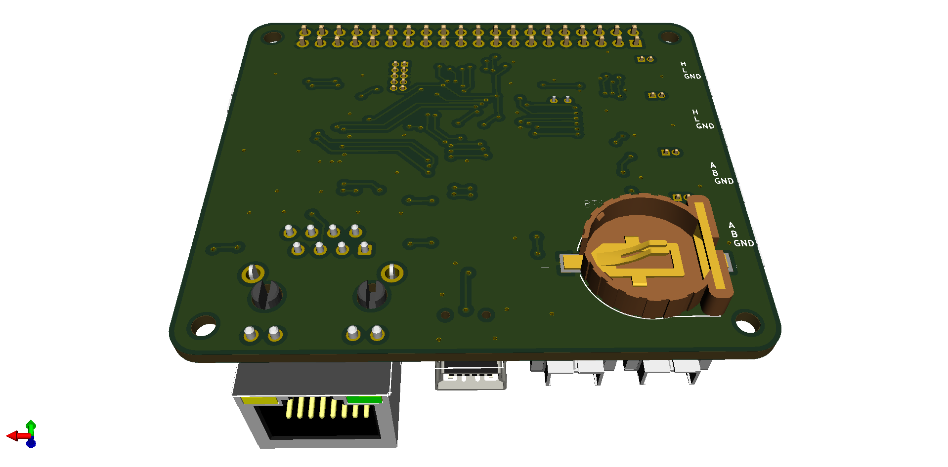
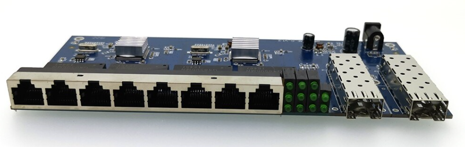
This is the schematics for Device-Bus, current sensor and power switch. I have a stripped down XPortHub that I might use for testing – removing W5500 leaves plenty of space without digging into 2nd side and 4 layer design. I simply would like to make some boards, put them in a stack and test for now.

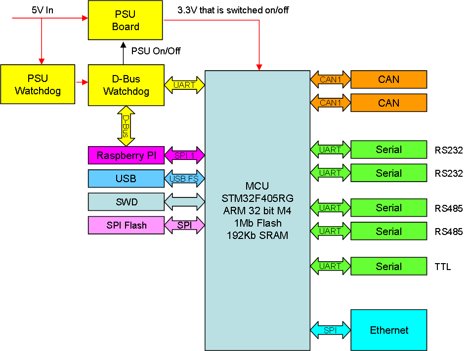
The challenge with using SPI’s in Half Duplex mode is that I need someone to be Master – to drive the TDM loop. This is a challenge as I start up without anyone assigned this task. I did consider several aproaches and decided on giving Raspberry PI a separate RPION pin it can pull high. RPI starts later than the others, and pulling RPION high will silence the bus – all devices moves to Device mode and wait for RPI to take over. This was the easy one.

The more complicated scheme is if RPI has not started or is not plugged in. At this point we will have several boards fighting over control. So I added a second BUSON pin which tells everyone someone is running the bus. I might use more pins here, but as a device starts it can wait a random time, if no-one switch on BUSON it can do so, wait a random time and if no-one start the clock it can do so. At this point we have used 2 x random number delays – it will take some bad luck for two devices to believe they have the bus, and even more to start the clock at the same time. To be sure we broadcast our uniue ID.

STM33G070 don’t have an unique ID and it don’t have a random number generator, but STM32F405 does so we use that one. The delays I talk about should be 1-100ms, meaning the entire start-up conflict should be settled in max 200ms if we have chaos – at normal start we have flags indicating what roles the devices have.

If we by some strange luck still have two Devices trying to control the bus we will just get garbage as we try to communicate. Each bus have resistors to avoid full short-cuts and we have current sensors that will detect pin short-cuts as well. So all we do is to drop the bus and start over again. Assuming we are master and lose communication we use the same scheme. It also means that if we unplug boards or shut them down someone else will take over the bus – it should work.

Once synched we need to figure out whom is on the bus so we can set up the TDM sequences – this time we have two of them. With two SPI-buses it would be tempting to run two schemes and accept that two different Devices control each their bus. This will however never work with Raspberry PI involved since the Broadcom SPI’s are more limited in the sence they only support SPI Half-Duplex Master.

My remaining challenge now is how do we detect that we are alone on the bus? Lets revert the question – the solution becomes more obvious as we ask for a list of confirmed Node’s we can talk to!

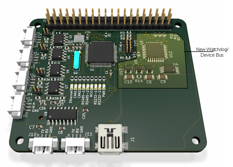
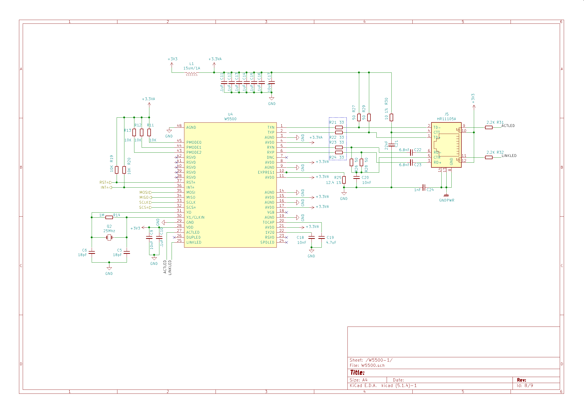
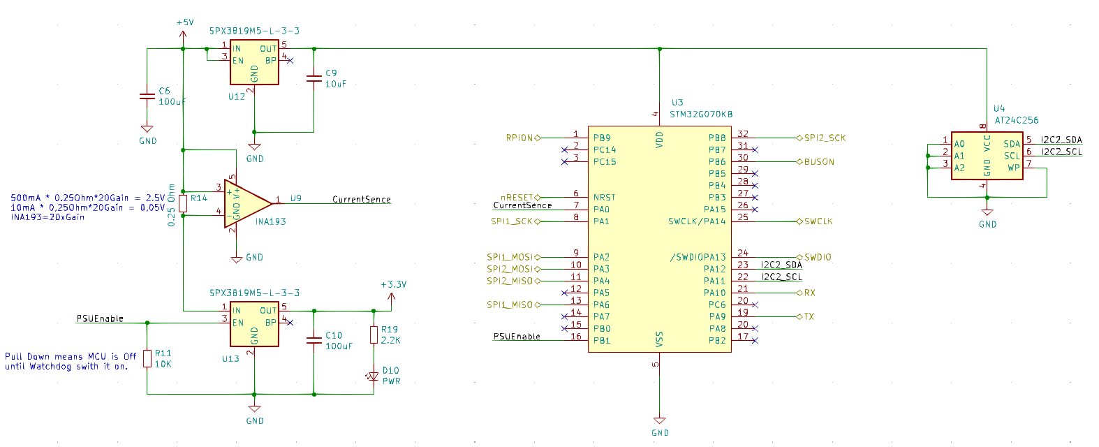
As for the schematics U12 feed 3.3V to U3 and U4 that is the MCU and EEPROM. U9 is an INA193 current sensor. The proposed 0.25 Ohm resistor will at 500mA produce 2.5V to the ADC and at 10mA 50mV to the ADC. I have to test shunt and gain later for a consolidated scheme – I am more interested in currents below 100mA than above, so lets see. I am a bit concerned that low currents will only be noise.

U13 is the power switch. On U12 we bind EN to 5V so that it is always on, but on U13 we connect EN to PA0 on U3 (G070). It has a pull-down so we are unable to switch power on before U3 does the job. This way we switch on G070 that switch on F405 (or not).

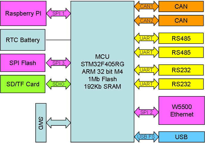
U3 is STM32G070KB. Part of the new M0+ series from ST and high spech at low cost. I was considering using a Flash page for data, but decided to add a low cost I2C EEPROM with 32Kb (258Kbit). This can store configuration for F405 as well solving another function I want on all boards. U4 is a TSSOP8 package and the I2C interface is 1Mbits/sec. EEPROM is slower to read/write than FRAM, but I am not sure I care. I can also add a CRC and write two pages etc to avoid havoc if we shut down during writes.

The UART connected on PA10/PA9 is capable of 6Mbits/sec and as we will be crossing TX/RX directly we will be using full duplex. We also have 7 DMA’s so we use 6 on SPI1, SPI2 and UART and still have 1 left for MEM to MEM. We also have 32Kb to use as buffers. I need to use interrups for EEPROM and bit banging for the ADC, but we have sufficient juice as this is a 64Mhz MCU.

Just a footnote that STM32G030KB is half the cost, only have 8Kb SRAM and 2 UARTS, but it’s UARTS are 8Mbps/sec. I2c’s and SPI’s are the same speed. I am having that in mind if we can downscale later. The entire BOM is below 3.- USD. It will take a while to order PCB’s and parts, but I am looking forward to this experiment.

Device Bus – Part 1

I was in the middle of planning a 8 pin bit-bang bus as my attention was drawn to STM32G070KB that cost 0.7 USD, comes in a LQFP32 package and contains: 2 x 1Mbps I2C, 2 x 32Mbps SPI, 4 x 6Mbps USARTS, 128Kb Flash, 32KbSRAM, running at 64Mhz and 7 DMA channels. Looking at the RPI pinout (above) this becomes very interesting.

So – what if I drop my bit-bang plans and use the two SPI’s for data transfer on the bus while I use a 6Mbps USART for communication with STM32 – basically dropping SPI between F405 and RPI bus? A 6Mbps full duplex UART backed by 2 x 32Mbps SPI’s is a lot of bandwidth.

Funny how things evolve – I started this by wanting to add an on/off switch to my boards – and we still have that as well – I also have several ADC’s and GPIO pins available on G070 so I have options in solving the tricky start up scheme. But, I need to draw sequence diagrams for the various situations to convince myself I have solved this.

I plan to use a I2C for a EEPROM storage. FRAM would be better, but it also cost more – lets see. A 32 Kb EEPROM also provide config storage space for F405 – so its far from wasted.

Moving on – I have space on top to add these components. My main concern is interference between the two MCU’s so this will force me up to 4 layers and components on both sides. I need ground planes between the MCU’s unless I manage to mount them on same side – but it is getting crowdy on some boards. SWD can be connected on RPI bus so we can program Device Bus. I am starting to like this concept 🙂


STM32 Flash Usage

STM32L011F4 only have 16Kb Flash, and as I generate the code I need from STM32CubeIDE it compiles to 11,37Kb on Debug, leaving only 4,63Kb Free for the application. Looking at the map I see several nasty C functions n the drivers. The GCC compiler is decently good and greedy on bytes, but that don’t help if the drivers use up the little Flash that is.

ST is great at Hardware, but their Software is not that great. It makes their small MCU’s non-usable if the driver uses all the Flash for itself.

My first idea was to use L011 as watchdog, but looking at Flash, SRAM and prices I decided to go for STM32G070KB that comes in a 32 pin package with 128Kb Flash, 32Kb SRAM and running at 64Mhz. This is a new M0+ series and I like the size and the price – buying from Farnell this time.

Watchdog/D-Bus

This is the block diagram for XPortHub2 with an added Watchdog/D-bus. My objective here is that I want to add some features to the board and decided to do an experiment adding an external Watchdog/D-Bus by using a smaller STM32 in support.

  • SPX3819 can be switched on/off enabling me to power a board on/off.
  • Adding a current sensor I also have an external watchdog in place.
  • I can use the Raspberry PI Backbone bus to drive a 8 bit SPI alike design to communicate with the rest of the stack.
  • I can communicate with STM32F405 using an UART.

The principle of a Half-Duplex SPI is simple as you run one clock and read/write data at the clock speed. Using 8 pins means I get 8x the speed of a single-line SPI and can achieve a high data throughput using a lower frequency. I want to test this on my new XPortHub2 and it only require a few, small components added. I probably have to re-route the entire board, but I think this will be worth it.

A Half Duplex SPI at 42Mbs per sec is ca 5Mb per sec – which is very fast. To compete with that I would need to bit-bang in 5Mhz speed. I don’t think that is possible, but 1Mhz should be realistic. Mhz here is Mb since we transfer 8 bits per clock. It is a lot of pins for an experiment, but I need a way for the Watchdog to commnunicate on it’s fun – so lets do this.

Adding a 2nd MCU at top using the bottom layer is doable, but it raises a chalenge – I will either need a breakoutboard for this or move to a 4 layer PCB to avoid interefence. I like the idea of a piggypack board for now – it is a less intrucive change on XPortHub – which by itself is going to require a change later regardless – I don’t expect to make a board as complex as XportHub and get it all right the first time.

XPortHub2 w/Ethernet

3D model of XPortHub2. This contains an 10/100Mbps Ethernet with a standard RJ45 socket that replace TF Card, I2C and SPI on XPortHub1.

  • New style SWD port.
  • Raspberry PI Backbone with SPI and CAN.
  • RTC with Battery holder on back.
  • 8 x user leds.
  • 2 x CAN ports. CAN1 is connected on Raspberry PI Connector so that CAN connect as you stack board together. Just like SPI.
  • 2 x RS485 ports.
  • 2 x RS232 ports.
  • 1 x USB port.
  • 1 x 10/100Mpbs Ethernet port.
  • 1 x TTL UART.
  • SPI Flash.

I fancied having a STM32 based board with Ethernet thought I already have an ESP32 based one. This board is attractive as a stand-alone adapter board as well.

Starting now we will also offer boards for sale. This is only limited number of prototype boards that can be purchased through www.basicpi.com.

This last image show the back of the board where you can see the CR1220 battery holder. One big upgrade is that KiCad show the ground plane correctly and even detect icelands. This groundplane worked out nicely.

SWD

J4 at right is the SWD connector. This can be reduced to 3 pins (SWCLK, SWDIO and GND), but it is wise to include Boot0, nRESET and 3.3V. I have painted SWCLK and SWDIO lanes in light red – those are the important ones that needs to be kept as short as possible. The only reason I use a 2×5 pin connector here is because they are easily available and give a stable connection base as I add a 1.27 pitch to 2.54 pitch adapter on top. It also gives the advantage that I actually can program the boards using a male adapter and just putting it down the holes. I recommend a proper connector if you work with the board, but this is a neat production trick to avoid mounting connectors on all boards.

This is my latest SWD format that I know apply on all boards, but I have so far used the same adapter board on everything and it have worked very well. I usually have a few ST-Link/v2 with adapters and it’s very easy to connect to board – which is how it should be.

I will however make a new adapter targeting boards inside a stack. I can manage with my existing ones, but I need to dissassemble the stack to mount/remove adapters. I want a new adapter where the PCB take me outside the board so I can mount/remove SWD’s while they are part of a stack.

Ethernet W5500 on XPortHub2 PCB


This pic is from the new XPortHub2 with Ethernet via W5500. The routing is close to being a single layer. The total number of passive components makes this occupy 1/3 of the board.

The only challenge here is that HR911105A is a bit to tall for the next board in the stack – this is not critical, but I will look for a lower profile RJ45. It is also easy to forget that silkprint takes as much space as the components on 0603 packages.

Fiber Modules

Fiber modules have been around for some years. The picture below show a 14.- USD 8 x Ethernet/2 x Fiber Mux/Switch that can be found on AliExpress etc. I have also seen smaller modules and 16 x Ethernet modules in the same price range – also boxed versions.

The interesting thing about these is that the Fibre links in theory can stretch a cable up to 100km. As I mentioned this has been around for decades, but it impresses me to see these modules down below 20.- USD in cost.

My own PLC uses high speed SPI as backbone and I already have Ethernet through Raspberry PI or ESP32 Board, but I fancied drawing a dual ethernet solution based on Wiznet W5500 as well. I have used this chip before. Ethernet and Fiber will extend the backbone to cover kilometers of wired net then needed. I am also a bit interested in using Ethernet as backbone all over, but space is a bit limited on the current Hat format. If I am to upgrade to Ethernet as backbone I will need to increase size, so having an Ethernet adapter is a compromize.

The ESP32 Ethernet module contains Ethernet and Wifi, but the SPI on it reduces backbone speed to ca 9Mhz as Slave. I can live with that, but I would prefer a higher speed. It is however challenges involved in using SPI the way I do, and a pure Ethernet backbone have a lot of advantages. But, is has one disadvantage – added space need on my boards + you need the switch in the backplane. And don’t forget that we also have CAN that can stretch over 1km.

Another option is to upgrade XPortHub and replace the SPI/I2C ports with an Ethernet port. I could just use magnets and a different, smalle connector etc. I have a bit of space problem here, but it can be done if I either sacrifice TF card or move TF card and/or battery to back side of card.